Meanwell NES Schematic..almost complete

NeilP

1 GW
Joined
Nov 27, 2010
Messages
5,012
Location
49.17303, -2.05354 Jersey, Europe
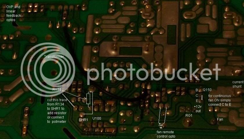
A schematic for the Meanwell NES series is almost complete now. Big thanks to Cor who traced the board out from my old one that I destroyed while trying a current mod.
It was one of the new NES series, and the mod was a bit experimental, needless to say I let the smoke out.
I posted it to Cor who has since done all the hard work of tracing the board of my dead one I sent him.
I have converted his drawing to a schematic in ExpressSCH

it still needs checking over for transcription errors from Cors drawing to Express SCH. After 12 hrs on it yesterday my eyes were getting a little tired.

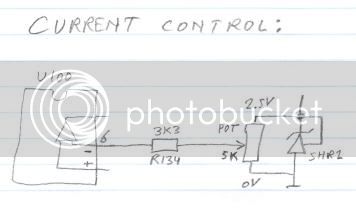
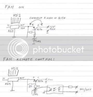
Cor has also worked out ways to mod it for current limiting..i'll let him tell you about that.

here is she schematic as it stands today.
I may yet re draw it to bring the Opto unit halves together ..unless someone else fancies that job ? If so PM me and I'll send you the sch file.


Edit


New schematic updated in light of corrections 26/1/12 ver 0.1
 

Attachments

  • NES 350-48 01 .bmp
    402.7 KB · Views: 6,004
Hi Neil,
Thanks for the hours you put in to get it into readable form ;)
For the FET, the answer to your question is in the FMH07N90E datasheet. :idea:
This shows type C with also the usual intrinsic diode from Source to Drain (though that diode is not used in this application).

One more mistake that I made in my sketch is that ZD2 on base of Q5 does not go to the ground as drawn, but to the negative input supply - the nearest point is pin 5 of U1 that has this connection.

I see that you have used just a single symbol for ground, while there are two different ground references and they are not connected: everything that is connected to the right side (secondary) of the transformer has the negative 48V output as reference, typically this is represented with a single fat horizontal bar but you might keep the symbol that you already use.
Everything on the primary side (left of the transformer, connected to the AC input) has the "frame ground" as reference since the AC input voltage can be floating. This frame ground (which is the actual alu case of the NES) is typically indicated with 3 flat bars underneath each other, each lower one is shorter so they fill in a triangle shape. You only need to correct this in 3 places: C3, C4 and the 4n7 cap under the two 680uF200V caps. And you can add a third input contact next to the 110/240V AC input, for connection of Earth ground. This contact you can also tie to frame ground.

The fuse is a fast-acting 8 Amp 250V AC standard size 20mm cartridge. The only thing different than usual is that it has a ceramic tube instead of the usual glass tube, probably to avoid it exploding and sending glass shards when something goes short circuit on the input, for example when a massive voltage spike (lightning strike?) hits it and protection ZNR1 tries to contain it or when C1 decides to short circuit. It is interesting that the PCB says:
F6.3AH/250V for NES-200
F8AH/250V for NES-350
while elsewhere on the PCB it is indicated that this board is NES-350-R1 2010/11/30 so not only is this a pretty recent design, but also it has leftover markings from the NES-200 design, which means that other NES (different power level) might have a lot of similarities to this design.

OK, we are on the home stretch here - these are the only cleanups that I could find. I will re-post my suggestions for current mods and the fan mod to get the 12V fan to run continuously, so we have all NES info concentrated in this thread.
 
OK, I drew up a few sketches about how to mod the NES-350-48 (should also work on other voltage versions) for current control
and for permanent FAN ON or remote fan control.
If you need a 12V supply then you can tap into the fan supply, but note that it is referenced to the negative side of the 48V output and do not overload this supply or you lose both the fan and the over-temperature protection!

Current control should allow turning the current down from the max specified to zero if you add a 5k (or 10K) potmeter across the 2.5V reference SHR1 next to the 8-pin U100 and connect the wiper of the pot to R134 instead of R134 directly connected to SHR1. The current through R134 controls the output current limit.
The SHR1 reference voltage (2.5V) is also used to set the output voltage, so do not overload this reference or the output voltage will go down.
You can set a lower current limit permanently without the potmeter by simply adding another resistor between R134 and SHR1. The value of R134 is 3k3 so adding a 1k resistor will reduce the current by some 25% while adding another 3k3 resistor will give you half the output current.
Currentcontrolschematic.jpg


The fan control can either be a permanent ON which is simply done by connecting the E and the C pins of Q150. This can be done with a short wire or a drop of solder. You can go fancier and make the fan remote control with either a switch or even an opto-coupler, for example if you want to control more than one NES which are in series, so their negative outputs are not the same level. you can add an opto to each NES and connect the LEDs to the same switch and power supply so you can control them together. SHR2 sets the reference level to turn the fan on, so the remote control can simply connect across this device to drive Q150 under remote control.
Fancontrolschematic.jpg


Here is how it looks at the bottom of the PCB - where to make the mods:
NES-350-48PCBbackcentercontrol-1.jpg
 
Great work guys. I'll try to go through the schematic and clean it up when I get a chance.
 
Just last night I started messing around with my NES power supply. I traced only the voltage feedback network and got dizzy...
Great job Cor and Neil! It will surly help with the MOD planned.

S.B.D
 
cor said:
This shows type C with also the usual intrinsic diode from Source to Drain (though that diode is not used in this application).


cor said:
One more mistake that I made in my sketch is that ZD2 on base of Q5 does not go to the ground as drawn, but to the negative input supply - the nearest point is pin 5 of U1 that has this connection.


cor said:
I see that you have used just a single symbol for ground,

Yes, it ws the first one to appear in the library on Express SCH :)

cor said:
while there are two different ground references and they are not connected:
Will change that


cor said:
. And you can add a third input contact next to the 110/240V AC input, for connection of Earth ground. This contact you can also tie to frame ground.

funny..It started out like that..but when i moved the input section from horizontal to vetical to fit on an A4 printout the input earth got deleted..i'll put it back for completeness


cor said:
OK, we are on the home stretch here - these are the only cleanups that I could find. I will re-post my suggestions for current mods and the fan mod to get the 12V fan to run continuously, so we have all NES info concentrated in this thread.

it would be nice to move it around a bit..so the halves of the Opto devices match up. I amy get around to that ,,but that is just the icing on the cake rather than any need for it

Will make a start now, before i go to bed
 
Neil,
I think you will find that if you try to move the optos together, then the rest of the schematic will become more convoluted,
since the optos are designed to straddle the barrier between primary and secondary side and maintain the galvanic isolation between input AC and output DC.
That is why I automatically split them up and just referenced them by their number so you can easily find back which affects the PWM controller in what way.
(that and the explanation that I originally gave in the previous thread that I think we should also link here "converting MeanWell power supply into LiPo charger" where the discussion about the traced NES supply starts with an explanation of how it works in post 299 and following, see: http://www.endless-sphere.com/forums/viewtopic.php?f=14&t=27199&start=299)
But I will await what you can do in aligning the optos, don't feel bad if the layout that was pretty nice and consistent with the optos split is not looking well once you tie the optos together... I like it when the schematic is organized in blocks of a certain function, such as V and I limit, fan control, PWM control and so on.
 
Done an update and replaced at the top of the thread

Cor, another few questions I amlooking at a few pics i took of the op of the board, input and output to the left, component side ..

the fast switching rectifier I destroyed..a single component, containing I believe two diodes..where is that on the schematic, on the board it would be top left when orientated as I say above


As for bringing the optos together..what I was looking at trying to do was still keep the 'blocks' of individual functions as they are, just re arrange each block, so the optos,are on the opposite sides of the 'blocks'so they 'pair up'

Not sure if it can easily be done yet but will look at it


Thats all for now, i am off to bed
 
Hi Neil,

See the secondary side D with snubber R100 and C100 across? That is one half of the high speed diode that you blew.
The other half is actually connected from the bottom of the secondary winding to the same +48V output as D, having R101 and C101 as snubber. I did not even bother drawing it because it should never be used since the bottom of the secondary winding can never get higher in voltage than the +48V output simply because it is directly connected to the negative 48V output (via L100). You can add it in the drawing but I don't think it will make a difference. For traceability it can make things clearer. You can also add the diode reference D100. (I have since revised my opinion and consider this diode necessary for buck-operation, see later in this thread)
 
is that high speed diode also called a schottky diode and have two anode legs and a single cathode leg? that is how i see the charge get pushed into the back end from the transformer on the chargers. and what does the snubber do that spans the diode? i was amazed at how hot that snubber resistor gets.
 
Hi dnmun,
Yes, it is often a Schottky diode (or pair of diodes) because the voltage drop (and thus the heat) of that type is lower.
The snubber is meant to dissipate quick changes in voltage across the diode, because the capacitor needs to charge up to follow the changes and the resistor is typically a low value around 10 Ohms or so, which means that a fast change of for example 50V will cause a peak of 5 Amps in a 10 Ohm resistor while charging up the cap. The reason to dampen these quick changes is to reduce radio emissions, because the changes are so fast (and the voltages rather high) that if not taken care of, the power supply can be a powerful broadband transmitter and you won't be able to listen to AM radio anywhere near the device. Another word for this type of operation is interferer and there are legal limits as to how much signal you are allowed to transmit, so in order to pass certification testing, the designer must reduce unwanted (spurious) emissions below the legal limits.
Another reason to apply snubbers on switching transistors and diodes is to protect the transistors and diodes from very fast rising pulse signals which might damage the part as well as the high peak voltage that may cause breakdown of the part.
The trade-off is a slightly higher loss due to the dissipation in the snubber resistor.
 
thanks for the explanation. i figured it captured the rf ringing when the conduction of the diode shut off and created some induction spike in the lead from the transformer. same thing... thanks alot.

i am getting a clone and will look at it and see how closely the circuit is related to the meanwell.
 
cor said:
The other half is actually connected from the bottom of the secondary winding to the same +48V output as D, having R101 and C101 as snubber.

Assuming we must be talking about the the negative side of the same (3rd coil ) secondary winding.

cor said:
simply because it is directly connected to the negative 48V output (via L100).

I thought I got that until you said


How is this? or should the anode of the lower diode go to the other side of L100

secondary.gif
 
cor said:
hi dnmun,
if you have a picture of the internals of the clone then it should not be too difficult to compare it to the NES.


Yea, need a pic of the clone. I have a Meanwell Clone that is exactly the same as a real Meanwell, yet there are others that are totally different..maybe this clone you have is the same as an NES..get the pic up and lets see...
Maybe post in the other Meanwell thread though.and try and keep this one just for the NES. Not so much for now, but threads that go off at a tangent can be a pain for someone trying to follow in future

http://endless-sphere.com/forums/viewtopic.php?f=14&t=27199&p=524160#p524160

or start a thread..link it back to here, dedicated to that particular clone, with info on where you got it from, exact name, and pictures etc.

We have a Wiki, now, once this Schematic and related info is complete, it should really be entered on there..You could maybe do the same with your clone. These threads get huge, go off at tangents and leave the newcomer totally lost and they end up asking questions that are on the forum..but buried in 50 page threads
 
amigafan2003 said:
On my NES-350-48 with it's trimmed shunt, when the current drops to 20ma it audibly clicks "off" and current ceases to flow. The led stays green though.

I generally charge with a turnigy watt meter inline so I know when it's "swicthed off".

Really ? interesting? When the relay trips out and it clicks off...the LED must go out as well? ...Oh , no, it won't will it...that power LED will be being 'back powered from the battery pack.

Maybe if Cor gets my dead one running he can confirm this does happen. and maybe find a way to alter the point that it kicks out. maybe get it to kick out at ..0.5 amps..0.25.A, and adjustable limit, to then save the need for an extra board

if this trip out point could be indicated by perhaps an LED ..coming on..going off, changing colour even better. Suppose to have an LED come on when the relay trips out would reaquire the LED to be powered from the AC side before the relay..Relay trips out LED comes on?
 
I'll add it in to the full schematic


With regard to R127 R128 I suppose they should really be shown connecting as close as possible to J100?
 
I partly tested the blown NES from Neil yesterday and also got the click, because I powered the U1 PWM controller directly with a power supply by feeding it directly into Q5. The output of Q5 sends voltage to the relay via a 510 Ohm resistor. If the output of Q5 rises to approx 15V then the relay pulls in (to short out the NTC resistor) and if the voltage falls to about 5V then the relay drops out with an audible click. Now normally the voltage on Q5 will never be around 5V because the PWM controller has a minimum operational voltage, I believe that below 8V it goes into standby mode.
Since Q5 is fed from the transformer - if there is no current that can be drawn from the 48V output then the voltage feedback will regulate the PWM controller back until also the other power supply outputs (fan, PWM controller) receive so little power that the supply goes into shutdown mode. That is why you hear a click from the relay dropping out and the supply shutting down.
Since the LED is across the 48V output, it will remain lit as long as the battery feed power back.
Simplest way to get an indication if the power supply is active is to wire a LED + resistor across the coil of the relay. It is supposed to get 12V, but take care as it is on the "hot" side of the supply (connected to AC) but having just plastic bulge from a LED sticking out of the PSU should not be a problem.
 
cor said:
Since Q5 is fed from the transformer - if there is no current that can be drawn from the 48V output then the voltage feedback will regulate the PWM controller back until also the other power supply outputs (fan, PWM controller) receive so little power that the supply goes into shutdown mode. That is why you hear a click from the relay dropping out and the supply shutting down.

Amigafan found it cut out at around 20mA, would it be possible , just by altering component values to change the point that it kicks out? or is that going to be easier done with the 3 pot Fechter/Goodrum board.

Schematic updated on post No.1
 
Yesterday I tapped to the OVP pad on my NES power supply. I connected one terminal of a 10k resistor to the OVP pad and the other terminal to an external lab power supply (also sharing grounds between them).
I wanted to see what voltage range I can get by feeding a voltage between 0-5V from the external PS. While playing around with the external voltage I also heard the relay kicking in and out.

My motivation is to see if it is possible to control the output voltage of the NES with an MCU to create a CCCV power source without tapping to the current limiting circuit (always staying below this level).

Is the purpose of the relay just to short circuit the current limiting NTC after the large input caps slow charge?

S.B.D
 
Cor, where on the Schematic is the OVP point as printed on the board?

SBD..check the schematic on first post of the thread..The relay chops power to pretty much the whole board.
 
Susbribed. Well done Neil and Cor- you guys are doing an excellent job!
 
Hi Neil,

I did have a look at it, and to my understanding the relay in normally open when mains power is applied. After the large input caps (2 X 600uF)charge slowly through the series resistor, the LDO ( Q5 ,ZD2 and the 3.9K resistor) can source the power for the relay to close, in order to short the resistor and allow larger currents to enter the power supply.

I don't think this relay cuts the input power completely, because if it is normally closed , a mandatory condition to start the circuit, and you want to cut off the input power (changing the state to open) you don't have a voltage on the circuit to keep it open....the system will start to oscillate.

S.B.D
 
Back
Top