Paralleling MOSFETs and IGBTs?

sa2tms

100 µW
Joined
Oct 20, 2017
Messages
9
Hi, first post on here. Got wind of this place existing from marcos' VESC variant being featured on Hackaday.

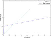
Anyway, a thought struck me the other day: IGBTs are good for higher currents due to their limited voltage drop. But there is also an almost constant bias to this drop, which is a disadvantage at lower currents. MOSFETs have the opposite properties - almost entirely linear I/V curve when fully saturated but higher voltage drop than similarly priced IGBTs at higher currents. So a thought occurs: why not parallel them? Both are driven the same way, typically have similar gate capacitances and voltages etc.

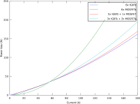
I decided to whip up a quick thing in Octave using numbers that fit two simplistic models to numbers in the datasheets for IXXX110N65B4H1 (used in the IGBT_board.pro KiCAD project) and IXFX100N65X2 (reasonably priced, low Rds(on), Vds >= 650V). Idea is we can populate a PCB like IGBT_board with six devices. How does the total power loss vs current vary with how many MOSFETs vs IGBTs we have? See attached figures.

As you might expect, one trades efficiency at higher current draws for efficiency at lower draws. Unless you just keep adding devices of course, and then it's just a question of BOM costs :)
 

Attachments

  • fig1.png
    fig1.png
    9.7 KB · Views: 830
  • fig2.png
    fig2.png
    20.2 KB · Views: 830
And the Octave code for anyone interested:

Code:
% Voltages to derive currents for
VI = 0:0.01:1;
VI2 = 0:0.01:1.15;
VM = 0:0.01:1.5;

% IXXK110N65B4H1 model
function V = v_igbt(I)
  % Mostly linear model with an exponential dropoff toward 0V @ 0A
  % Kinda stupid, but seems to follow Fig. 3. Output
  % Characteristics @ T_J = 150ºC well enough

  % Very little conduction until around 0.5 V
  Vth = 0.5;
  % Looks to be around 1.9V @ 100A
  % R = (1.9 - Vth) / 100;
  % "At 30A, 0.9v Vce = 27W per transistor"
  R = (0.9 - Vth) / 30;

  % Exponential term
  k = 5;

  V = R*I + Vth*(1-exp(-I*k));
endfunction

% IXFX100N65X2 model
function V = v_mosfet(I)
 % Worst case = Fig 3. Output Characteristics @ T_J = 125ºC
 % Be even more pessimistic by not accounting for the lower
 % resistance at lower currents
 R = 6.7 / 100;
 V = R*I;
endfunction

% Inverse of v_igbt
function I = i_igbt(V)
  Vth = 0.5;
  R = (0.9 - Vth) / 30;
  k = 5;

  % Initial guess
  I = V / R;
  % Newton's method
  h = 0.1/k;
  for x = 1:100*k
    I = I - h*(v_igbt(I) - V)./(R + k*Vth*exp(-I*k));
  endfor
endfunction

function I = i_mosfet(V)
  % Trivial
  % Avoid defining R twice be calling
  % v_mosfet with I=V and dividing away V
  I = V./(v_mosfet(V)./V);
endfunction

% Show models
% Base model has voltage as a function of current,
% But current as a function of voltage will be useful further down
figure(1);
plot(i_igbt(VI),VI, i_mosfet(VM), VM)
xlabel('Current (A)')
ylabel('Voltage drop (V)')
legend('IGBT model', 'MOSFET model')

% P/I curves for different configurations
II = 6*i_igbt(VI);
IM = 6*i_mosfet(VM);

IMIX  = 5*i_igbt(VI) + i_mosfet(VI);
IMIX2 = 3*i_igbt(VI2) + 3*i_mosfet(VI2);

figure(2);
plot(II,    II.*VI,
     IM,    IM.*VM,
     IMIX,  IMIX.*VI,
     IMIX2, IMIX2.*VI2)
axis([0,180,0,250])
xlabel('Current (A)')
ylabel('Power loss (W)')
legend('6x IGBTs','6x MOSFETs','5x IGBTs + 1x MOSFET','3x IGBTs + 3x MOSFETs')
 
sa2tms said:
IGBTs are good for higher currents due to their limited voltage drop. But there is also an almost constant bias to this drop, which is a disadvantage at lower currents. MOSFETs have the opposite properties - almost entirely linear I/V curve when fully saturated but higher voltage drop than similarly priced IGBTs at higher currents. So a thought occurs: why not parallel them?
A few reasons:

1) Twice the gate drive losses, twice the parasitic (D-S) losses.

2) They don't share. On resistance of MOSFETs goes up with temperature - which means you can parallel MOSFETs and they will share quite well. IGBTs have their ON voltage go down with temperature, at least at lower currents - which means they don't share well. As a single IGBT gets hotter, it draws more and more current, until it is very hot and taking almost all the load.

(That means if you parallel MOSFETs and IGBTs, the IGBT will end up taking most of the current.)

That being said, an adaptive system (where the system switches from MOSFET to IGBT at some point) may be worthwhile if you have to design a system that has a very wide voltage range.
 
billvon said:
sa2tms said:
IGBTs are good for higher currents due to their limited voltage drop. But there is also an almost constant bias to this drop, which is a disadvantage at lower currents. MOSFETs have the opposite properties - almost entirely linear I/V curve when fully saturated but higher voltage drop than similarly priced IGBTs at higher currents. So a thought occurs: why not parallel them?
A few reasons:

1) Twice the gate drive losses, twice the parasitic (D-S) losses.

This I've anticipated. I have a potentially very clever or very stupid idea for reducing gate drive losses that I'm going to post so no asshole goes and patents it: bounce the gate charge to/from an inductor. Use this inductor both for charging and discharging the gate. Don't bother with a gate resistor. Keep the inductor current topped up to whichever charge/discharge current you need. Use an ideal diode to freewheel when not needed. Unless I've completely brainfarted on the physics this should keep the switching energy from being turned into heat as in a normal driver, apart from ESR losses of course. See attached KiCAD sketch (not pictured: oodles of voltage/current sensors, op-amps and switching logic).

file.php


Some critical things: L1 would need to be air wound or maybe a PCB inductor in an 8-32 layer board (thick copper, very wide traces, not overly many turns). Not sure if much can be done about D-S losses however. Maybe Cds could be discharged into the inductor before switching the device on?

billvon said:
2) They don't share. On resistance of MOSFETs goes up with temperature - which means you can parallel MOSFETs and they will share quite well. IGBTs have their ON voltage go down with temperature, at least at lower currents - which means they don't share well. As a single IGBT gets hotter, it draws more and more current, until it is very hot and taking almost all the load.

How do you even manage this with IGBTs then? Sounds like you'd have to monitor the current going through each one very carefully. Or stay out of that troublesome range..
 

Attachments

  • driver.png
    driver.png
    6.2 KB · Views: 1,071
I wouldnt worry too much about gate driver losses, it could be 1 or 2 watts in a 10 kw system.
More imporant are switching losses in the drain/source while the half bridge is switching from 0 to 400v for example. That I×V do make a difference, and is easy to optimize by driving harder the gate and making the switching sharper. There is a limit of course given by the di/dt that your layout allows. And then there is how good your current sharing is between your paralleled devices,there are IGBTs out there that behave well in parallel applications.

A Model S has 14 IGBT in parallel, I wonder how that plot looks like.
 
marcos said:
I wouldnt worry too much about gate driver losses, it could be 1 or 2 watts in a 10 kw system.
More imporant are switching losses in the drain/source while the half bridge is switching from 0 to 400v for example. That I×V do make a difference, and is easy to optimize by driving harder the gate and making the switching sharper. There is a limit of course given by the di/dt that your layout allows.

di/dt? Not dV/dt? As I understand it the main limit to switching is the resulting dV/dt on the gate potentially causing damage. Seems most drivers use a constant voltage + series resistor to the gate. So gate current drops as gate voltage increases. Plus a long time is spent in the Miller region. This seems kind of dumb to me when an op-amp could potentially overcome this. This sketch hopefully shows my thinking (zero effort spent drawing in any kind of compensation):

driver2.png

Ideally the gate voltage would rise with a constant dV/dt that is as high as one is comfortable with, right? My idea is you apply that square-ish signal to CTRL.
 
sa2tms said:
This I've anticipated. I have a potentially very clever or very stupid idea for reducing gate drive losses that I'm going to post so no asshole goes and patents it: bounce the gate charge to/from an inductor.
That's resonant gate drive. We use that for our very high frequency (>2MHz) inverters.
Unless I've completely brainfarted on the physics this should keep the switching energy from being turned into heat as in a normal driver
What gets you is the Miller capacitance, which will prevent that from working as well as it seems like it should. But it will still reduce gate drive losses.
How do you even manage this with IGBTs then? Sounds like you'd have to monitor the current going through each one very carefully. Or stay out of that troublesome range..
A few ways.

1) Don't parallel them. (There are some VERY large IGBT's available these days.)
2) Keep the load in the region where the imbalance is either zero or in the right direction (tough to do with motor inverters tho)
3) Ballast resistors, which work great but of course increase losses.
 
billvon said:
sa2tms said:
This I've anticipated. I have a potentially very clever or very stupid idea for reducing gate drive losses that I'm going to post so no asshole goes and patents it: bounce the gate charge to/from an inductor.
That's resonant gate drive. We use that for our very high frequency (>2MHz) inverters.
Aha, "resonant gate drive" are the magic words to search the literature for. Thanks :]
Seems gate drive losses indeed start to dominate as switching frequencies go up.

billvon said:
Unless I've completely brainfarted on the physics this should keep the switching energy from being turned into heat as in a normal driver
What gets you is the Miller capacitance, which will prevent that from working as well as it seems like it should. But it will still reduce gate drive losses.
Good to see my mental model is sensible at least. Dumping enough charge into the gate to get past the Miller region as fast as possible would be quite a challenge.

As I suspected none of these are novel ideas. Darn!
 
Back
Top