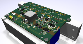
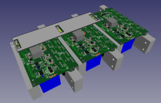
OSHW TO247 IGBT watercooled laminated half-bridge

marcos said:
Njay said:
What PWM frequency are you planning on using, Marcos?
20khz at most. I'll probably use lower than 10khz

you mean 21kHz. keep the switching frequency as a value evenly divisible by 3 and this will magic out some harmonics
 
I have to calculate an approximate gate resistor value, and check the gate resistors power rating is okay..

gate resistor, keep in mind that its value has profound affect on performance of switch and so you don't really want it to change value due to self heating. also, gate resistors are netoriously hard to cool because the floating nature of the gate drive reference means you really don't have a cooling path to ground. these two things mean you have to oversize the watt rating of the gate resistor. calculated you need 0.5W, the 1W minimum is what you use. for example.

I was worried that this driver doesn't support cycle-by-cycle 2 step turn off, it only does a soft turn off during a desat fault.
personally that's what i like. i do not want cycle-by-cycle.. only 2-step after desat. i recommended cycle-by-cycle to newbies because they don't typically understand that at elevated power levels the parastics cause desasterous levels of voltage transients so you have to LEARN by hard knox methods to build the geometry of your power pass paying attention to 3D fields and interconnect parastics. that's hard to do for newbies so i recommended cycle-by-cycle... rather it works than not. but if you have a good handle on the more difficult parts than going maybe cycle-by-cycle you don't need.

Is a separate turn OFF gate resistor enough to limit di/dt slew rate? I want to avoid the inductive spikes while switching off the igbt, not sure if a simple gate resistor will do the trick
OFF resistor is one method. mostly though the di/dt is driven by your switch and your capacitor's ability to deliver energy.. mosfet/igbt are all made differently and some switch faster than others for otherwise the same system. really, you don't want to switch too fast.. fast is good, less losses, but too fast is bad, high EMI. its all about a balance. basically what i do is pick quality parts, especailly for the switch i have only trusted manufacturers that i use, build the power pass to good geometry and then i say "well, did the best i could" and then i only play with the gate resistor ON/OFF values to get the switching characteristics that i want which is basically just a balance between getting good efficiency while within EMI limits. i talk a lot of theory.. but in practice i just bang it out on the bench like everyone else ;)
 
HighHopes said:
you mean 21kHz. keep the switching frequency as a value evenly divisible by 3 and this will magic out some harmonics

In order to do this, wouldn't the PWM need to be generated with 1Hz accuracy? That could be asking a lot from the controller.
 
not sure what you mean. we program for 21kHz instead of 20 kHz. or 18kHz instead of 20khz. 18, 21 .. both evenly divisible by 3. so your question is will the processor be stressed if it tries to generate a 21kHz frame rate as compared to a 20kHz. or 18khz as compared to 20khz. so here we are talking about 1000Hz resolution.. not 1.

the frame rate is divided down from your system clock which is your oscillator which is probably fixed frequency like 8MHz, 16 MHz, or 150MHz. none of these would suite well to 21kHz PWM frame, true, but i think its not a problem because the system clock is more than 100x faster. having said that, you are asking for the timing & scheduling of a processor.. this i am not an expert at so i could be wrong. i can tell you that when i wrote the spec for such resolution i never got questioned about it so i assume it was never a problem to the programmer ;)
 
HighHopes said:
marcos said:
Njay said:
What PWM frequency are you planning on using, Marcos?
20khz at most. I'll probably use lower than 10khz
you mean 21kHz. keep the switching frequency as a value evenly divisible by 3 and this will magic out some harmonics
That short sentence got me into a lot of reading, and I still don't understand it. Going through several papers, all I got is that fc/fm should be multiple of 3.

fc/fm = 3k ,( k ∈ N )

That is carrier freq (i.e. PWM freq) divided by fm, or fundamental freq (which would be proportional to the electric RPM). Attached what I found about this.

So, fixing fc to 21khz doesnt fix fc/fm to a multiple of 3 because fm is proportional to the motor rpm... what am I missing?


About the controller capabilities, its no problem to generate 21khz. You often have 16 bit timers, PLLs and prescalers, with my case of 8MHz crystal I multiply the internal clock up to 168 MHZ. Some of the timers only work at up to 84MHz.

So, with 84MHz and a period of 4000 clock cycles I get 21000.00 hz, with 4001 clock cycles it would be 20994.75hz, so thats about the resolution you get in a mcu. (PWMfreq = clockfreq/period)
 

Attachments

  • spwm.pdf
    59.8 KB · Views: 143
HighHopes said:
I have to calculate an approximate gate resistor value, and check the gate resistors power rating is okay..
gate resistor, keep in mind that its value has profound affect on performance of switch and so you don't really want it to change value due to self heating. also, gate resistors are netoriously hard to cool because the floating nature of the gate drive reference means you really don't have a cooling path to ground. these two things mean you have to oversize the watt rating of the gate resistor. calculated you need 0.5W, the 1W minimum is what you use. for example.
Good, I put 4W gate resistors. I used zombiess sheet to calculate that I need 2W at 18khz. Will add copper planes and vias around resistors to improve dissipation as much as I can.
HighHopes said:
I was worried that this driver doesn't support cycle-by-cycle 2 step turn off, it only does a soft turn off during a desat fault.
personally that's what i like. i do not want cycle-by-cycle.. only 2-step after desat.
Great to hear.

HighHopes said:
Is a separate turn OFF gate resistor enough to limit di/dt slew rate? I want to avoid the inductive spikes while switching off the igbt, not sure if a simple gate resistor will do the trick
OFF resistor is one method. mostly though the di/dt is driven by your switch and your capacitor's ability to deliver energy.. mosfet/igbt are all made differently and some switch faster than others for otherwise the same system. really, you don't want to switch too fast.. fast is good, less losses, but too fast is bad, high EMI. its all about a balance. basically what i do is pick quality parts, especailly for the switch i have only trusted manufacturers that i use, build the power pass to good geometry and then i say "well, did the best i could" and then i only play with the gate resistor ON/OFF values to get the switching characteristics that i want which is basically just a balance between getting good efficiency while within EMI limits. i talk a lot of theory.. but in practice i just bang it out on the bench like everyone else ;)
Yeah, you're operating in expert-mode, driven by experience which is a lot more practical, I just have the theory and big ears to listen to the experts :D. Its a similar design flow across ee, you choose solid parts, solid theory, and then you debug it until it comes together, because it never gets spot on in the first try.
I read somewhere that is difficult to calculate gate resistor value accurately, so I was already planning some trial and error to find a right value.

Thanks for the input guys
 
bigmoose said:
A while back when working on a water cooling system for TO 247 FETs I was looking at a 1/4 inch to 3/8 inch thick by 1 inch or so wide trip of aluminum furnace brazed to a 1/4 inch or 3/8 inch water/antifreeze tube tube. I like to add one drop of surfactant to the coolant (think Dawn dishsoap). Just an idea to consider if it meets your heat transfer requirements.
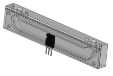
Thanks. I drafted a simple heatsink that I can mill here. No turbulent flow, no fins to reduce machining time, no fea simulation, no thermal simulation, just a bunch of water flowin near the transistors
file.php

The part is in the same github repo, I just want to make sure it wont leak even under high liquid pressure, there are good sealants for that. Anyway, liquid cooling is the last thing of a long development, I'm not even heating transistors right now, but it helps to have the mechanical supports in mind, and that heatsink is important support-wise because ibgts are clamped to it, pcb and copper sheets are aligned to it, etc. Its subject to change though, its only a first draft.
 

Attachments

  • heatsink.png
    heatsink.png
    37.3 KB · Views: 2,618
zombiess said:
What material are you using as a dielectric between the pos and neg bus and how thick will it be?
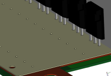
I'd like to use 0.8mm bare FR4 without copper. FR4 has 20kV/mm, so it would provide adequate insulation.
With a sheet like that I can drill it to align tightly the igbt, film caps and copper layers, so it serves a dual purpose.

file.php


Maybe I can go down to 0.4mm, I made a few thousands of 0.4mm pcb boards and they are reliable, I'm just not that confident working at +400 V in a shaky environment with small cleareances.
 

Attachments

  • insulation.png
    insulation.png
    11.5 KB · Views: 2,618
A couple of notes that HH pointed me to:

I don't see snubber caps on your first page. i would like to ssee them direclty across your phase leg. don't show it with your DC link caps, put the 1uF snubber cap right across teh IGBT leg in the schematic. Placing like this in the schematic is like a reminder that the snubber cap needs to be as physically close to those phase leg DC+/- connection as possible

Um, I acually don't have snubber caps. Well, I do. See, there are seven 16uF film caps at 10mm of the IGBTs, with a really low Z path. I don't know if I should call them snubbers or very good dc links. And I can fit 7 caps for 6 IGBTs, so the schematic looks odd when I put one cap per igbt and then place another seemingly random cap in there. Zombiess suggested an extra 100uF cap that I'm trying to figure out how/where to fit, that would be an actual DC link.
caps_location.png
Those caps are in the schematic as a reference, because they aren't actually installed on the PCB, but directly across the copper bus bars. Its a bit of a stretched integration between EDA and the CAD.


HH also made me question the series diode D1 in the gate drive circuit, and it made no sense, I copied it from TI eval board. That diode adds dispersion and a tempco, and you can already control ON/OFF separately without a diode.

i see just one NAND gate in your schematic. look at my schematic for the PWM overlap elimination circuit and make sure yours is the same.
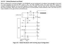
Your overlap circuit behaves as mine, because when the NAND is active it triggers the FAULT signal. This signal mutes all the driver logic of the 3 phases, and can be detected from the MCU. The mute mechanism is by driving IN+ low. Its the same mechanism used to mute the driver in case of a desat event, the only difference is that a desat fault latches the muteing until a reset is asserted.

When operating in inverting mode (connecting the PWM signal to IN-), driving IN+ low is suggested in the datasheet to mute the driver, there is an schematic example.

global shutdown.png

reset.. careful noise doesn't cause this thing to give you speratic if the uC is far away or has connect inbetween. maybe pull down needed?
The driver IC has an internal pullup resistor. I added a couple of nF to make it more stable without delaying the reset signal too much.

transformer T1, you winding this yourself? you need to keep the primary/ssecondary capacitance to <10pf
Not a chance, its an off the shelf part that I took from a TI eval board. http://www.mouser.com/ProductDetail/Wurth-Electronics/750342312/?qs=s%2FuNXRgw4gTNpp0LsKECVg%3D%3D
Datasheet doesn't specify its capacitance though.

TP10 and other test points on the gate driver.. careful these things act like antennas. prefer to have NONE
Noted. Removed! Bad timing, I was almost getting used to follow IPC2221 suggestions about testpoints.
 
HighHopes said:
not sure what you mean. we program for 21kHz instead of 20 kHz. or 18kHz instead of 20khz. 18, 21 .. both evenly divisible by 3. so your question is will the processor be stressed if it tries to generate a 21kHz frame rate as compared to a 20kHz. or 18khz as compared to 20khz. so here we are talking about 1000Hz resolution.. not 1.

the frame rate is divided down from your system clock which is your oscillator which is probably fixed frequency like 8MHz, 16 MHz, or 150MHz. none of these would suite well to 21kHz PWM frame, true, but i think its not a problem because the system clock is more than 100x faster. having said that, you are asking for the timing & scheduling of a processor.. this i am not an expert at so i could be wrong. i can tell you that when i wrote the spec for such resolution i never got questioned about it so i assume it was never a problem to the programmer ;)

If the Fsw is set to 20.001 kHz, it's divisible by 3. At 21.001 kHz, it's no longer divisible by 3. This is why I'm asking if 1Hz resolution matters.
 
I've been thinking about adding a way to control the overshoot, by changing the negative gate control voltage, which originally was fixed at -8V.

I saw this mechanism in a tesla patent, and seemed like a fairly doable way to get control over the overshoot and switching losses. So at low phase currents we can drive the gate very hard with less switching losses, and at higher currents we can drive it softer to avoid DC bus overshoots.

The control should come from the controller (duh) across the isolation as a variable frequency, then converted to a voltage, then used to control a voltage regulator. I've been suggested to pay close attention to the gate resistors, but those -8v were unregulated, and that can throw away all that effort. So, regulator it is.

Something not trivial in that chain is the frequency to voltage converter. There is a chip that does that with a very high linearity, but ultimately it relies on an RC circuit, and I don't like at all capacitor tolerances. IMO a better way is to put a small MCU to read the frequency and use its DAC to control the voltage.

And if I put an MCU, I get an ADC for free, so I can read voltages like Vgate, Vce, and power supplies. And there is the internal temperature sensor for free. All this is of limited use, with the ADC I can measure only every 150nsec, no chance to see high freq stuff, and its impossible to transmit such information over the isolation. But it could be useful to have an idea of the amount of overshoot and send it back to the controller. Oh, internal sensors are crap, but hey, its free.

I'll keep thinking, I chose a 5x5mm MCU I'm familiar with, an isolator, and roughly simulated the voltage control.
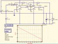
dac_control_simulation.png

Maybe I'll only use the ADC for Vce (its just connecting the MCU to the copper sheets below). Measuring Vgate would be interesting, but I'm adding an antenna to a critical track. Also, its not a rad hard mcu, so I don'w want to mess around with many tracks. Keep it simple, just digital in, digital out, DAC and 1 analog in easy to route. I'm a bit worried about the noise immunity of those opamps though.
 
marcos said:
So, fixing fc to 21khz doesnt fix fc/fm to a multiple of 3 because fm is proportional to the motor rpm...

i don't know how much thoery you want in an answer but the the short of it is that fundamental and carrier frequency are not periorid in synch with each other. its a common misconception this fc/fm triplen harmonic ratio. the ratio does not lead to harmonic reduction.

D.G. Homes, author of the book “Pulse Width Modulation for Power Converters: Principles and Practice” writes:
The popular misconception that it is a triplen
carrier/fundamental ratio which causes carrier and sideband
harmonic cancellation between phase legs appears to have arisen
from early harmonic analysis work which assumed an integer pulse
ratio and a general harmonic form. …the error is in the use of the
general harmonic form, which implicitly assumes a 0° phase
relationship between the reference waveform and the carrier. This
relationship is not sustained for the other two phase references
unless a triplen carrier ratio is defined, so that the application of
the general harmonic form is only valid for a triplen carrier rather
than requiring such a ratio.
 
marcos said:
I've been thinking about adding a way to control the overshoot, by changing the negative gate control voltage, which originally was fixed at -8V.

this is a lot harder than it sounds. if i were you i would put this on your "to do" list for revision 2. it not necessary to have for a functional motor drive, its just nice to have. there are enough problems to solve to get something to work properly at your power levels than to worry about the subtle of this feature.
 
HighHopes said:
D.G. Homes, author of the book “Pulse Width Modulation for Power Converters: Principles and Practice” writes:
The popular misconception that it is a triplen
Yay! Thanks for looking it up HH, I'll give it a try.

Today I figured out its a ton easier to integrate a variable duty pwm with RC than to convert freq to voltage. No clue why I came up with the frequency approach. So, no mcu needed.

Having -VEE regulated vs having -VEE controllable from the controller only adds an opto, opamp and transistor. I might lay it out since it wont interfere with the gate driver layout.

While learning about this I found some bad things in my layout regarding current loops of the gate driving path, will change that soon.
 
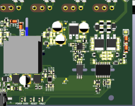
Changed the layout a bit for more symmetry and better placement of the caps next to transistors.

driver layout.png

Also, I decided to go 4 layers in order to have better current loops management, and to lower the gate tracks impedance. Its not that expensive when you factor in how many layout hours you save, the components cost, and cost of a failure.

One particular benefit is that I can lower the impedance of the gates track. Its a long track, and each nHy along that track will delay the signal, so the closest IGBT will turn on/off sooner than the last one.

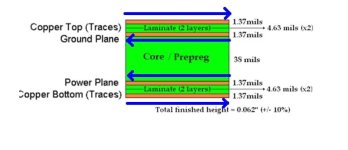
The pcb manufacters I worked with so far tend to use very thin laminates (~0.15mm) in the outer layers and a thicker (0.8mm) FR4 as the middle layer, roughly like this
stackup.jpg
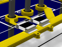
So I can use that to have the gate current and gate return current only 0.15mm apart, one on top of the other. And twice, because there are 4 layers. Can't model asymmetric layer stackup in kicad... yet.
4_layer_gate_track.png
I'm aware that those vias can act like antennas, but I think that less inductance is more important.
 
agreed the cost is not prohibitive, but don't go more than 4 layers.

One particular benefit is that I can lower the impedance of the gates track. Its a long track, and each nH along that track will delay the signal, so the closest IGBT will turn on/off sooner than the last one.
the nH here is small... so small in fact that you might be able to get equal nH if you change the width of the tracks to compensate...

i haven't spent enough time llooking at your layout to put it fully in my mind but i see you dropping vias to pickup 4 layers of return current or something like that. you probably going to need at least 3 vias for that per resistor.. not one.

on your mosfet plated through hole, be mindful of the creepage between pads. some are high voltage, some are low voltage..

this is really good work marcus, keep it up.
 
HighHopes said:
agreed the cost is not prohibitive, but don't go more than 4 layers.
Yes, 6 layer boards turned out to be a bit finnicky in my experience, had some non negligible warping due to power planes design.

HighHopes said:
the nH here is small... so small in fact that you might be able to get equal nH if you change the width of the tracks to compensate...
If I keep those traces not very wide I can ultimately use a thinner heatsink. That means less aluminum to mill, a more adequate heatsink, and confortable cleareances. A too wide track will couple to the phase copper sheet underneath the pcb. I try to keep all those things in mind, but I didn't went though the numbers yet to sort out what matters and what not, I'm just in general layout stage right now.

HighHopes said:
i haven't spent enough time llooking at your layout to put it fully in my mind but i see you dropping vias to pickup 4 layers of return current or something like that. you probably going to need at least 3 vias for that per resistor.. not one.
Agreed

HighHopes said:
on your mosfet plated through hole, be mindful of the creepage between pads. some are high voltage, some are low voltage..
Yes, I made a custom footprint without soldermask in the HV IGBT pads, will have slots between pins when I get the time to do it.
 
the nH here is small... so small in fact that you might be able to get equal nH if you change the width of the tracks to compensate...
Trying this random calculator found online, I get 110nHy with a 1.6mm thick pcb with 2mm traces that is 11cm long.
Using this 4 layer/thin laminate approach I get 5.2nH, thats ignoring the series inductance of the vias I have to use. Those vias don't add to the inductance difference between IGBTs, its equivalent to leg inductance.

To get a value that low only by increasing width, the trace width would be 4cm wide, picking dV/dt. Using a 1mm thick pcb would need 2.5cm trace width.

This is because those layers are surprisingly close to each other. Thats also why you want to make the first inner layer a GND plane, it gets very close to the smd components on top.

So its more than tenfold decrease in inductance. Is it relevant? I don't know, but its free :)
 
zombiess said:
If the Fsw is set to 20.001 kHz, it's divisible by 3. At 21.001 kHz, it's no longer divisible by 3. This is why I'm asking if 1Hz resolution matters.
I THINK this advice comes from the guys who are running things on mains power. What you want is a multiple of three of the net frequency. If you're not going to tow a long extension cord behind your car, this is not an issue for you.

That said.... The system crystal will be +/- 50ppm or 1:20000 already. And the net frequency can change by as much as 1:50... That said... Doing say 400Hz switching might be bad because you'd do the same switch in the same phase of the line frequency every time. But once you're doing say 10kHz switching, you'll be switching at every phase in the line frequency, so you're always spreading things evenly.
 
i think we were talking about two different things. the harmonic stuff is related to the carrier frequency only in a 3-phase AC motor drive. 10kHz is pretty low, there are pros and cons of switching frequency selection.. generally you want to stay between 15kHz to 30khz. you can go higher and you can go lower, but you should have a good reason to do so. there are many implications to think about. what i do is design the system to accept in that range. except for the AC filter if you have one, that i wait on until i picked the frequency to use. sometimes the design starts out with a plan to use only 60kHz, or only 3khz that's OK but there is a reason.. but if you don't have a reason to be specific its good to leave yourself a range so you can have some opportunity to optomize notice all values i mentioned were devisable by 3 ;)
 
I wont comment about fc/fm stuff until I find the book...

In the meanwhile, I added phase voltage sensing
phase sensing.png

Schematic sheet is here
https://eyrie.io/board/c5ac1a5f21ce4684914535b2669bd01a?active=schematic&sheet=6&x=6492197&y=4218298&w=14165749&h=7656809&flipped=false

Next stop is the non-isolated side of this board (bottom of the image), and see if I want to change the connector. I ran out of pins.
Then start thinking about the location of the VESC brain and 3x bridges assembly.
Review the layout by as many people as possible
Copy the gate driver layout of the right (low side igbt driver) to the left side (high side driver)
Try milling a copper sheet
 
Only added a few bolts to support the board and changed the connector for a 12pos header.

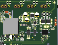
board.png

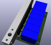
Here is a 3D view, its a bit troublesome to update, I won't publish it this way very often.
https://skfb.ly/XZzD

And trew it in the cad to see how the 3 phases look together with a brain board on top of a metal shield.

inverter1.png

I think I'll push -VEE to -12v. Right now is at -8v and for this power level is probably short.

Also I'm learning about kapton/nomex paper/kapton to keep DC bus as tight as possible.
 
HH,
what is the rationale behind using external logic gates to avoid a destructive shoot through pwm signal?

The logic that shuts down the output when both top and bottom PWM are active is built in the gate driver IC. Both your infineon gate driver and my TI gate driver have the same input logic:

input_logic.png

It seems that connecting PWMtop and PWMbottom like you did in your driver, would cover the case of a logic shoot trough, without the need of external logic. It makes for a simpler and more reliable circuit.


I guess the external logic won't add any relevant amount of added time when you calculate the total deatime required, but I still don't quite understand why the logic redundancy.
In my board there is the added benefit that the controller would know if a logic shoot through happens (it asserts the FAULT signal while both inputs are high)... but I don't see any like that in your schematic.

I was going to remove the protection logic, but I thought I should ask first, maybe I'm missing something.

Merry christmas folks
 
Marcos, I believe the reason for the external circuitry is to address a fault before it occurs. It seems more relevant to a design that uses separate High/Low gate drives vs one that has them both integrated into a single chip that has a lockout type function.

Highhopes also uses that input technique of making the PWM input signal differential which greatly improves noise immunity. It's quite clever. I've never met someone that has thought through failure modes so well. He really stressed that type of thinking to me while teaching me gate drive design / layout. Always know how the circuit behaves during a fault, then test the fault modes on the bench. While it adds design time and additional parts, I've managed to build 4 gate drive / power stage designs and every one of them performed much better than someone with as little power electronics experience as I had could have ever hoped for.
 
zombiess said:
vs one that has them both integrated into a single chip that has a lockout type function.
What do you mean by lockout? I mean, how is the external logic different than the internal logic?

zombiess said:
Highhopes also uses that input technique of making the PWM input signal differential which greatly improves noise immunity.
Thats exactly what I want to do, if I remove the logic gates I can run differential, length matched, via-shielded, controlled impedance traces from controller brain right up to the driver pins, like I'm doing with the phase voltage sensing. I cant do this that far if i have discrete logic gates messing with the signal path.
 
Back
Top