CellLog 8 hacking

fechter

Administrator
Staff member
Joined
Dec 31, 2006
Messages
16,536
Location
California Bay Area, USA
There is quite a bit of information in an earlier thread: http://endless-sphere.com/forums/viewtopic.php?f=14&t=12815

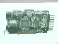
I recently got a couple of CellLog 8M units for testing. The 8M is similar to the 8S, but much cheaper and does not have a logging funtion or USB interface.
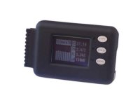
CellLog 8M product photo.jpg

Here is the User's Guide:
View attachment CellLog 8M.pdf

Of particular interest to me was the layout of the power supply inside the CellLog.
The current drain of the CellLog is such that if you always left it connected to the pack, it will drain the cells fairly quickly and somewhat unevenly. My goal is to find a nice way to turn it off without unplugging it.

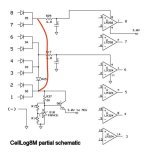
The front end/ power supply arrangement is interesting. There are diodes on each input the direct voltage to a linear regulator that supplies 3.0v to run the MCU and display backlight. The MCU is an Atmel ATMega32.

Cells 1 and 2 feed their voltages directly to the MCU through some resistors.
The remaining cells go to differential amplifiers that take the difference between inputs and reference them to ground for direct input to the MCU.

Cells 3 to 6 go into a LM324 quad op amp that is powered by a feed from the diodes on those cells.
Cells 7 and 8 go into a LM358 dual op amp that is powered from the diodes on those cells. Since the LM358 has a maximum supply voltage of 32v, they put the power ground of the LM358 to the 3v supply instead of to ground. This gives it a little more 'headroom' in the voltage rating.

By disconnecting pin 0 (pack -) connection, the unit can be largely turned off, but the op amps are still draining the cells to some extent.

Here's a partial schematic showing the power distribution inside the CellLog: Not shown are the input resistors going to the op amps. Also note: the op amps are not necessarily shown in the right order.
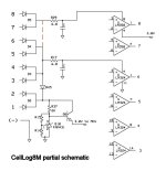
CellLog 8M front end schematic.jpg

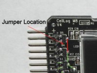
The dashed red line shows the location of the jumper needed to 'even out' the current drain on the CellLog as figured out by guys on the R/C forums.

Without the jumper, cells 1-6 will be drawing more current than 7 and 8, resulting in unbalanced cells over time. By adding the jumper, the drain is more evenly distributed on the cells.

Here are some shots I took of the board. It's really hard to trace the circuits because the solder mask is black. If you hold the board up to the light at just the right angle, you can sort of make out where the traces run.
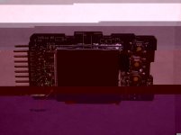
CellLog board top.jpg
(Click picture to enlarge)
CellLog board bottom.jpg
 
With my CellLogs I installed a mini switch on lead wire #1 and left it turned off for a week. I don't remember the voltage lose after the week but it was so small I felt safe to use this process. I guess your correct in what you are saying so I would think that leaving a pack with the CEllLog turned off in my method could and would draw down the pack when stored for the winter. I guess I'll just pull the CellLogs for long storage. Without question the switch is quick and simple to install and it's a lot safer then constantly unpluging it. Beside the same switch turns on my alarm out put add on alarm. Flip the switch and everything come alive. Bob
 
Toorbough ULL-Zeveigh said:
do u feel it wud b worth the effort replacing the op-amps with ultra lo-power versions?

I suspect it wouldn't help that much.
Jumper Location.jpg

With the jumper installed between D4 and D5, the current draw when powered is around 20ma @32v.
If I lift the pack (-) and run 28v from cell 1 to cell 8, I now measure right around 500uA. This is not too bad.

The only thing is the first cell won't have any drain at all but the rest will. A cheezy way around that would be to add about a 7.5k resistor across cell 1 to equalize the drain.

I think I would be OK with that amount of drain. For extended storage, I would still recommend disconnecting the whole thing.

Even if I were to lift the 3 spots where power feeds in and run them off a separate switch, there would still be about 70uA of drain from the input resistors on the op amps, but I don't think it would be worth the work. It would be really cool if the guys that make the CellLog had some kind of switching arrangement that would allow remote turn on and turn off.

I also tried out the sleep mode. It is essentially useless. 20ma on, 13ma sleep. I'm not sure exactly what is sleeping, but I do see the backlight turn off and the display goes blank. Looks like everything else is still powered up.
 
In looking at it a bit more, I really don't see why they didn't install that jumper. The only disadvantage I can see is there will be a little more heating on the voltage regulator transistor and slightly higher drain.

I think they should make it "standard equipment"

Fortunately, it is very easy to install.

Since the LM358 is rated for 32v max, and has a 3v boost on the ground, pin 8 should never be allowed to go above 35v. The manual states 42v or something, but I think that only applies to using the pack level jumper clips supplied with the unit.
 
Assuming you are going to use the full 8S compliment, (and please remember I am no engineer)... wouldn't these:

http://www.st.com/stonline/products/literature/ds/1536/uln2805a.pdf

Work perfectly (well for up to 7S per IC) and is about 1.00 each, needs 5v supply and some can pass 50v max (who needs it... 32 is about our max at 8S right? - also perfect region for LM317)

-Mike

PS: Yes I am suggesting we use these as disconnect switches to keep it low power and solid state... the current drawn by the CellLogs is totally adequate for this and the voltage drop is calcuable as .03 + .03 = .06 (I think) of the input voltage for offset calculation through the dip.
 
I was thinking of using opto couplers to switch the 3 voltage inputs. This could drop the drain down to about 70uA when off. If we want to use more than 8s, it is necessary to isolate the switches or at least level shift them.

Anything that goes between the batteries and the CellLog will affect the readings. A mechanical switch or relay won't be an issue, but pretty much all solid state devices will introduce a significant voltage drop. They make analog switch chips that use FETs that might work.

Doctorbass found a mechanical relay with enough contacts to do it, but I think the relay would be several times larger than the CellLog (and draw more power).
 
And speaking of isolation....

The alarm output connections and USB connection on the 8S are NOT isolated. They are referenced to the pack (-) connection.

If we want to use more than 8s cells, we need to have the outputs tied together, but they need to be isolated or level shifted. I think you're out of luck on the USB ports though. They would work fine one at a time, but to use more than one at a time would require some kind of USB port isolator, which sounds expensive if it even exists. Maybe a wireless USB adapter? Why not make it Bluetooth?
 
Isolating the USB port can be done... the same way I used to isolate the Serial TX/RX coming from the Atmega32L onboard... I tapped it before the CP2102 chip but.... there is no reason we can't power an optocoupler on the output stage and using a 2 channel high speed, manage to transmit the USB data along via isolated output.

This would be on another PCB obviously or inbuilt to the USB cable used between them...

ANother option (one I've used a few times) is to actually opto isolate a 4 port USB hub, much much cheaper than buying an isolated hub for stuff like this :)

Since we really only care about receiving USB log data (right?) from multiple units... The easiest way is to marshall all the TTL level (direct Atmega tap or use teh test points on the PCB) serial would be to connect up to 3 Cell Log8s up to a single Atmega1280 (they have 4 ttl level serial uarts)... optocoupled this allows you access (at a rate you can program) to each line of what normally just comes over USB->Serial anyway...

Final output is then concatenated and redirected out the 4th uart which is run through a single TTL->USB chip - now you haev up to 24S of ability... (this is based on Arduino Mega)... if you skip the arduino parts... then you are free to use all 4 of the UARTS (Arduino has a TTL->Serial USB on UART 1) for receiving data so now we can do 32 cells... then you will need one USB->TTL and some simple serial bit banging to output the data via a digital pin (software serial libararies work fine for transmit just receive can be goofy with timing).

The final trick is linking an opto coupled bus to engage the Start Logging button via a digital output line on the Atmega (which goes to all the slave CellLog8s) which is held high (turned on) for 3-4 seconds on power up to begin the logging output via TTL :)

-Mike
 
fechter said:
With the jumper installed between D4 and D5, the current draw when powered is around 20ma @32v.
If I lift the pack (-) and run 28v from cell 1 to cell 8, I now measure right around 500uA. This is not too bad.

fechter said:
I think I would be OK with that amount of drain. For extended storage, I would still recommend disconnecting the whole thing.

To put this in perspective, if you have a 10Ah pack, and a .0005A discharge rate, it will take 20,000 hours to drain the pack dead. That is 833 days, or about 2-1/4 years. Even if the pack is only half-charged, that is still over a year. I just think it is pretty nutty to talk about reducing the drain by a factor of 7, when it is already not a problem, unless you plan on going into deep space, and need to hibernate for 16 years. :roll: :)
 
fechter said:
Toorbough ULL-Zeveigh said:
do u feel it wud b worth the effort replacing the op-amps with ultra lo-power versions?

I suspect it wouldn't help that much.


I also tried out the sleep mode. It is essentially useless. 20ma on, 13ma sleep. I'm not sure exactly what is sleeping, but I do see the backlight turn off and the display goes blank. Looks like everything else is still powered up.

I think the only this that is tured off is the screen. So why not just call it a screen saver? Aside for the small amount of power savings I like the idea of turning off the screen. After all who is going to look at that little thing when your riding.
 
I really like the little critters. Would be cool to be able to put your name on the startup screen and change the music at startup to "dixie"?

Its good to hear how long i should have b4 pack damage. The cellog wires 2-8 is the only thing connected to my pack during "storage" . it will be in fact permanently soldered on . So I guess I should be looking for cell one to be high then? Balancing will only be periodic, im hopeing every 50 cycles or so, mabye once a month. I wont mind losing a bit of range due to imbalance mabye %10. So I think it will be acceptable.

Keep it up! I could alos mention that I have changed the output transistor of the alarm , with a large npn mounted outside of the case. now i run a big relay no problem at alarm. i had to do this because i blew my alarm outputs right away with tomfoolry!
 
OK, I can see an issue with the D4-D5 jumper... this will expose the LM324 to full pack voltage and it's only rated for 32v. This means if you exceed 4.0v on HVC, it will be over the limit. Not a problem for LiFePO4, but maybe a bad idea for Lipo.
 
Getting in an reprogramming them is rather trivial. AVR programmers can be had for cheap. You can develop code using the free WINAVR package which has a full GCC compiler.

The main problem is finding out the specs on the LCD/controller chip. It looks like a cell phone display. Finding out what LCD controller it uses can be difficult. They are usually a chip-on-glass device covered with a blob of epoxy. Once you have that figured out, you need to trace the pins back to the AVR chip and locate the pads used to program the chip (It programs via the SPI port).
 
It has number on it. I'll try to see what it is.


OK, I think I figured out a "have your cake and eat it" solution to the diode jumper.
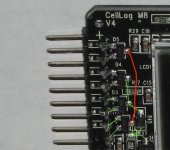
If we connect the output of D5 directly to the regulator input, we can avoid feeding full pack voltage to the LM324. The regulator input can handle over 40v. In this configuration, the drain on cells 7 and 8 should be pretty even with the rest, and the maximum voltage should be 35v (8 x 4.375v) which should be high enough.

Installing the jumper is a bit more difficult, but not too bad. It looks like this:
CellLog 8M jumper 2 schematic.jpg

Location on board is here. Note: there are several other possible attachment points that are all connected on the bottom side. Use whatever is easier.CellLog Jumper location 2.jpg
 
Thanks Fechter! It is really convenient to have and electronics "genius" around when you need one!

otherDoc
 
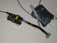
After messing around for a while to get the USB drivers to load, I got my AVRISPmkII to connect to the CellLog.AVRISPMKII+CellLog.jpg

After connecting, I was able to read the Flash and EEPROM sections of the MCU.

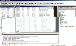
Here's a screen shot of the AVR interface:
AVR studio screen shot.jpg

This is compiled code, so it's pretty hard to make out what's going on in there.
At least I have copies of the code so I could reload it in the event the CellLog memory gets corrupted.
I sifted through the code but did not see the "do not support the logging" text anywhere. I suspect it is not stored as text in the code but is a graphic image.

Unless there's a way to uncompile the code, there's not much hacking I can do with it.

If anybody wants a copy of the downloaded code files, let me know.
 
Did you ever find any info on the LCD? If we can figure up what LCD/controller is used, one can completely rewrite the code from scratch. I saw some info that the LCD is a 128x64 graphic LCD. I have quite a bit of AVR/LCD interfacing experience. I wrote the code for the Mega-Donkey LCD libraries.

I doubt the "no logging" message is a bit map. That takes quite a bit (1K) of memory. The mega32 only has 32K of flash.
 
I have a unit with a broken screen, that still works otherwise , if anybody wants to test it for magic smoke particles !!! my friend was at the vendor, showing the kid that works there the bike. He managed to do the --rednecks famous last words. "hey ya'll watch this", and landed on the cellog. also broke some bottles in my backpack !! fat bastard

pm me the address and ill mail it ....
 
One thing that concerns me with the display on these is that there are 30 pins on the LCD interface. Almost all LCD's with a controller chip on board have 14-20 pin interfaces. Those with more pins are usually naked LCD modules that can be very difficult to work with. That said, the MEGA32 only has 40 pins. Almost half would go to power, ground, clock, ADC inputs, switches, etc. That leaves enough for a standard LCD controller interface, not a raw LCD interface.

I looked around for some LCDs that looked likely and didn't see anything that looks like whatever they are using.
 
I didn't get a chance to take a real good look at the LCD. It seemed pretty naked though. Definitely a lot of the pins on the processor go to the display. I left it at work so it will have to wait until next week.

So if a bitmap is bad practice, then I should expect to find that startup text somewhere in the code, but I didn't see it in plain english. It's a HEX file and I used a hex editor program to scan it. It is very long, so I may have missed it. The disassembler in AVR Studio seemed to have a bunch of the expected kinds of commands, but I don't know enough about how all that stuff works to tell what the program is doing.
 
The LCD display does not have a lot of markings. On the ribbon cable, there's a barely readable set of numbers.
It looks kind of like MGA356DMN3W. The first 3 characters are not fully legible, especially the second one. Could start with MBA, or M6A?

Second line has: MM1003081

I do not see any embedded chip on the unit. All wires seem to go back to the MCU.
 
Back
Top