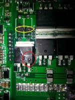
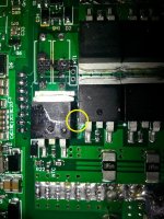
What resistor value is this (16S ANT BMS)

pwd

10 kW
Joined
Oct 11, 2011
Messages
799
Location
Ontario, Canada
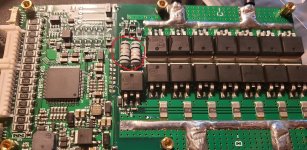
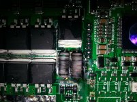
My burnt resistors on a ANT 320A 7S to 16S BMS from IC GOGOGO on AliExpress:
IMG_20200623_165804.jpg

I found an image of the same board but im not sure if it has the same current rating or if that matters:
74ca3be74665a9babb0393879f96f4b5dc6e4248_2_1380x776.jpeg

According to https://www.digikey.ca/en/resources/conversion-calculators/conversion-calculator-resistor-color-code-5-band

I end up with 50.8 Ohms but I want to double check; since sometimes my eyes don't see colour that well.
 
The ones on your board (burned) I can't tell what they used to be.

The ones on the ohter board, well, those colors don't match the standard for 5-band resistors.

The color bands on the parts are
Green
Black
Silver (definitely looks silver, not gray)
Gold
Black

If for some reason they made them using silver paint instead of gray, then that would match a standard color code value, and you could use that resistor to replace it.


I can't find the component designation in the silkscreening of the PCB, but if it starts with an L instead of an R, they are inductors rather than resistors, but 5-band colors on those should have a doublewide silver band at one end, so the colors on these don't match the standard either.


You could try measuring the ones you have (removed from the board), to see what they read as. If they read correctly, then you don't even need tore place them (though you would want to find out what other part in series with them has failed to cause them to burn, since resistors don't burn like that unless there is some other problem in the circuit, unless it is a very bad design not using a sufficient-wattage part).
 
I went looking too, I don't know anything about this stuff but I read silver and gold meant high voltage? but this link says +5% +10%

https://www.allaboutcircuits.com/tools/resistor-color-code-calculator/
 
Yes, but not at the 3rd band. That one doesnt' get a silver or gold in a 5-band code.

On these components, whatever they are, the third band is silver, no matter which end you start from, and that isn't a standard color code on any parts I've seen.

If they accidentally used silver paint instead of gray, then the value the OP got from the first calculator is valid.

If not, and it's actually supposed to be silver...then it doesn't fit the standard.
 
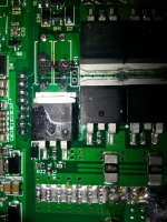
Thank you both for you analysis so far. I've removed the items and have cleaned up the board as much as I could:
IMG_20200624_181325.jpg
There is a marking on the board near the resistors that appears to say "RT1".

The resistors (or whatever they may be) are in even worse shape on the underside. One measures ~ 55K-65K ohms and the other is jumping around 200K-250K ohms (I can't seen to get a solid reading on either).

The silver band (is it supposed to be grey) and black band at the end is throwing me off too...

for the record, the board was working fine until some water hit the board. The bluetooth function still worked. Last time I plugged it pack into the pack; the pack voltage was correct but it said something like "discharge mosfet abnormality".
 
pwd said:
There is a marking on the board near the resistors that appears to say "RT1".
That's for the pads next to the marking, for a thermistor, a temperature sensing resistor, probably specifically to sense the temperature of those resistors and the FET next to them, specifically to prevent this sort of problem, but omitted from the design because it saves a few cents and the board "works" without it, at least until whatever occurs that causes the overheating condition.

If you knew what type of thermistor was designed to go there, you could add it, and the software may have the function still in there (just disabled by default), or it could be a hardware-only function, whcih may require other components elsewhere on teh board that may or may not be populated.


The resistors (or whatever they may be) are in even worse shape on the underside. One measures ~ 55K-65K ohms and the other is jumping around 200K-250K ohms (I can't seen to get a solid reading on either).
Neither is very surprising--severe overheating can destroy the component, or just damage the resistive (or inductive, etc) element, *or* just damage the interconnects between the element and the ends. And the heating is worse on the bottom because it's trapped and reflected by the PCB surface and traces underneath it.


for the record, the board was working fine until some water hit the board.
"some water"? Specifics and details may help determine the cause of the fault and let you fix it (though no guarantees).

FWIW, if I had this probelm, and had any choice (could use the pack without it till I could replace it or coudl use a different pack) I wouldn't even continue using it if it had water damage, especially if it caused a fault with it. You don't know what hidden damage (corrosion, etc) that may be lurking in PTHs and under SMT components, waiting to cause a fault that kills your pack or leaves you stranded.

If the pack itself also had water damage, I'd consider the entire thing suspect and keep a very close eye on it forever, even if you can't *see* anything wrong now.

Last time I plugged it pack into the pack; the pack voltage was correct but it said something like "discharge mosfet abnormality".
You'd have to trace it out, but I'd guess that those resistors are in series with the discharge FETs, being used as some form of shunt resistor for current sensing. If they are instead supposed to be gate resistors, then if they got that hot there's something wrong with the drive circuitry too.
 
amberwolf said:
If you knew what type of thermistor was designed to go there, you could add it, and the software may have the function still in there (just disabled by default), or it could be a hardware-only function, which may require other components elsewhere on the board that may or may not be populated.
Interesting, the other temp sensors that get plugged into the board are 10K NTC. I may try adding one after I get things sorted out.

amberwolf said:
Specifics and details may help determine the cause of the fault and let you fix it (though no guarantees).

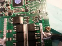
The full story is that I was riding and it started to rain which became a heavy downpour. The battery enclosure wasn't water tight around the discharge cables and I suspect the water entered from there. When I removed the panels/heat sinks from the BMS, I noticed some water droplets around the FETs. Here is the area where I think the water caused the issue, you can see a white residue:

IMG_20200625_083500.jpg
IMG_20200625_083422.jpg

There was a tiny ball of solder in between the two mosfets on the end. I have tried to remove most of it. Maybe the two mosfets were momentarily bridged together because of the water? I'm not sure if the solder ball was the result of them getting hot and causing the solder to melt. You can see the white residue between the two last mosfets. I've seen that before on other electronics with possible water damage but don't know if that is a definite sign.

I have ordered a new BMS and plan on removing the heatshrink and rubber padding to inspect the pack connections and cells. It would be nice to be able to get this BMS working again; just to say I did; even if I don't use it.
 
pwd said:
The full story is that I was riding and it started to rain which became a heavy downpour. The battery enclosure wasn't water tight around the discharge cables and I suspect the water entered from there. When I removed the panels/heat sinks from the BMS, I noticed some water droplets around the FETs. Here is the area where I think the water caused the issue, you can see a white residue:

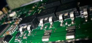
FWIW, the FET whose tab is connected to the pads the resistors mount on appears to be different in texture, which may simply be conformal coating, or it may be heat damage. There is a small square-looking line that may be a crack in the plastic where the smoke came out, and a round dimple between it and the leg. Circled in red in the attachment.

Circled in yellow is wha'ts left of the silkscreening that gives the burned part designation. I can see a "1" but not the rest of it.
IMG_20200625_083422.jpg

That FET may be shorted in a way that causes high current flow (though I am not sure how it could have anything other than normal flow, without shorting thru other things that would destroy other things on the BMS, feeding thru cell sense wires, etc).

Still, you can test that FET to verify it is open circuit with the BMS disconnected from the pack, and that it is closed circuit when it it is connected to the pack and the pack is in a state that that FET should be closed circuit.

I'm guessing it is the charge FET?

The water could've bridged the gate to a voltage sufficient to turn the FET on, but that shouldn't have caused a problem because it should *already* have been on, even if it was the charge FET.


There was a tiny ball of solder in between the two mosfets on the end.
Where exactly was the ball?

If it was on the tabs, they appear to be electrically connected anyway.
 
amberwolf said:
FWIW, the FET whose tab is connected to the pads the resistors mount on appears to be different in texture, which may simply be conformal coating, or it may be heat damage. There is a small square-looking line that may be a crack in the plastic where the smoke came out, and a round dimple between it and the leg. Circled in red in the attachment.

Good eye. There definitely appears to be a crack (although very small) on the mosfet you've circled in red. Too bad the part designation was burned.

amberwolf said:
Where exactly was the ball?

The ball was located here:
IMG_20200625_083422_2.jpg

I've attempted to test the mosfets using diode mode on my multi-meter using this method (first time I've ever used diode mode and the mosfet pinout was different than the one he was testing):
https://youtu.be/gloikp9t2dA?t=83

I tested all of the mostfets with the BMS disconnected from the packand they all appear to be open circuit *except* the one in question on the end/with the crack. That is giving me a reading of 0.013V in diode mode.

So maybe it is the mosfet that blew? I still don't have a good idea of what the resistor values were. I went to a local (small) electronics shop and they figured the the board with the un-burnt resistors (I showed them the photo) was only 0.5 ohms. That didn't seem correct to me but they would know more about components etc... than I would. I got them to order a couple; just in case.

I'm actually feeling pretty good about this troubleshooting; which is requiring me to stretch my knowledge. I appreciate all your help.
 
Something still had to cause a high enough current draw to overheat the resistors, and to blow up the FET.

Without knowing what that was, they may fail the same way again once replaced. :(

If you trace out the circuitry from the FET and resistors to power and ground, you will see the current path, and the things that control the stuff that is in the current path. Then you would know which things could cause current to flow in a different path that could become uncontrollable, or in the wrong direction, etc. It's not necessarily easy/simple to find the cause of this kind of failure, especially when it's an environmental intrusion (like water) that can remove it's own evidence (evaporates), so you dont even know all of what was affected--only what you saw directly, and wherever deposits/corrosion/etc is left behind (which won't be everywhere it got to).

If those parts are the charging circuit, rather than discharge, then they have a limit to the current they are designed to handle. But there isn't a path anywhere I can think of to cause them to flow current beyond that limit, except while charging. So if they failed while discharging, and no charger was connected/active, it would be difficult to see how current could be forced to flow thru them, which is the only way they can be overheated like this.

If the solderball managed to *solidly* connect the discharge fet's discharge-port connection to the charge fet's charge port connection, then the charge fet would be paralleled with them, and share their current flow. But it's probably a cheaper higher resistance part than the discharge fets, if it is a different part (I'd expect them to use the same ones to decrease part count purchases/increase volume). So it should have less current flow thru it, and not heat even as much as the discharge fets, and not overheat. But...if the discharge fets were already handling say, 20A each, and the charge fet is only meant for say, 5A, then even if it began passing only 10A, that's twice as much as it was meant to, and probably beyond the design capacity especialy since it would already be heated indirectly from the discharge fets' heat passed thru the PCB to it.
 
Back
Top