monster
100 kW
- Joined
- Jun 17, 2007
- Messages
- 1,411
Hi
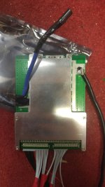
I'm repairing a bike for a friend. He has given me all of the components including this BMS which seems to be mislabeled.
Normally i would expect to see connections for B- (battery -ve), C- (charger -ve) & P- (controller -ve).
Sometimes there is only B- and -ve.
On this board there are three solder tabs but the little one is marked P- and one of the big tabs is marked P- on one side but C- on the other side. Where the P- and the C- are connected.
Sould i connect as a 2 tab BMS and ignore the small P- tab,
or should i assume the small tab is a mislabeled charger tab and use the big tab for power even tho its marked C- on one side?
Has anyone else used a BMS like this?
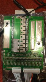