My new 18 FET TO-247 layout riding video page 10

zombiess

10 MW
Joined
Jan 31, 2011
Messages
3,048
Location
Oklahoma City
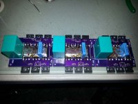
This is a new layout I've been working on so I don't have to use a shoebox sized case. This one is also more powerful as it utilized 3 parallel IRFP4568's. Current sensors will be HASS 600A units. I'm now working to scale down the Lebowski controller board so it will fit in the case below these boards.

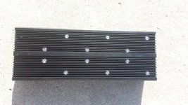
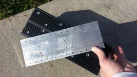
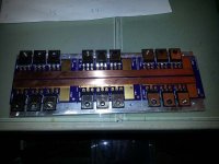
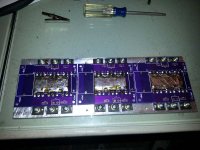
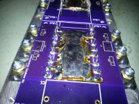
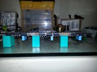
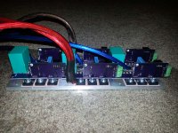
The phase output boards are individual. Masking has been removed from the top and bottom layer in the proper location so that I can run 0.375 wide 0.125 thick copper buss bar for the bat+ and batt- connections. The FETs are mounted face down and will be attached to a 3.5" wide 10" aluminum bar stock which then attaches to a Hammond 431623 enclosure which is 11.2" long. Phase output connections will be made by surface mounting 8 gauge wire to the bottom board, 2 strands if needed.

I'm not 100% sure if I should keep a G-S cap/resistor on each MOSFET or just run one single one right off the gate input. I like the idea of having just one G-S cap and one G-S resistor vs putting them on each MOSFET.

Battery connections will be made towards the center of the buss by the capacitor. I am extending out some of the copper buss bar and soldering the wire to it, probably 4 gauge. All the polypropylene caps are mounted on the bottom side of the board.

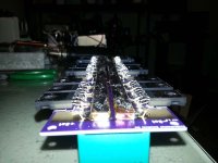
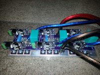
The gate driver boards are mounted at a 90 degree angle to the main power board and then attached by two 3 pin 90 degree headers which make electrical and mechanical connections. This is why the driver boards are mirrored the way they are, keeping everything symmetrical.

This is not final yet, but it's getting close unless I hit a show stopper. I need to get my first controller on my bike and riding, but this is following close behind as the other controller is just way too big for practical usage.

This design will be open source, but it's lacking the proper documentation right now. It's the same basic gate design as the original power stage I built and most of the components have the same numbers so the document in that describes many of the component functions. I also have a spreadsheet which helps you calculate the desaturation, timing and 2 level turn off components. This is going to take a while to document, but I wanted to put it up here and get some input / reviews.

You will need to have KiCad installed to look at the files. Some of them have a lot of layers and it's going to be the best way to examine the work so you can turn them on/off as needed. The output stage has 2 internal layers to create a laminated power buss, the internal layers don't carry much current.

I'll probably think of more, it's late.
Gate driver with 15A boost stage, 2 layer board
KiCad files View attachment 1
View attachment Driver With Boost V2 Schematic.pdf
View attachment 4


18 FET H Bridge, single phase, 3 required, 4 layer board
KiCad files View attachment One Phase.zip
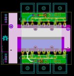
Output One Phase.jpg
 
nieles said:
what kind of caps will you be placing on the Vbus for the fast voltage peaks(close to the fets)? large ceramic caps?

pulse rated polypropylene. Snubbers are 1.0uF and the DC Link cap is 20uF.
 
ah yes i see them now.. just downloaded kicad! couldnt see them in the pictures.

Very nice layout!

about the copper pours (green layer above the fets) thats for low impedence right?

from what i have been reading, you should only connect the copper pour on one place,
otherwise large currents could be flowing through them.
 
nieles said:
ah yes i see them now.. just downloaded kicad! couldnt see them in the pictures.

Very nice layout!

about the copper pours (green layer above the fets) thats for low impedence right?

from what i have been reading, you should only connect the copper pour on one place,
otherwise large currents could be flowing through them.

Green layer is the bottom copper. It is the ground plane for the gate loop. Its purpose is to reduce noise coupling and provide a short return path. No idea about the impedance, goal was to keep the loop area small and not cross over the power pass sections.

Not sure what you are saying about the planes having multiple connections. I have not heard that before. I was told the gate connections to the power sections need to be done similar to how a kelvin resistance measurement is made and that it is vital to not have any gate components cross anything high power such as the DC buss or phase out. If something has to cross one of those sections it must be done at a 90 degree angle to minimize coupling.

The warning I received from high hopes on this design which does have me paying attention is that with the power pass sections all overlapping thermal management is important because its possible to burn through the board and cause a short. Initial prototype is being made with 1.6mm board, 1oz top/bottom copper layers and 0.5oz internal. If this works well and I go to production I will have thicker boards produced to minimize this risk. All internal layers are low current.

I believe I have a very good thermal path due to my aluminum plate sink everything mounts to. It is 10" long, 3.5" wide. Not sure how thick I can go until everything is in hand, but I hope to run 0.25". If that does not work I have 0.187" which should. I drew a basic 2d design in AutoCAD to figure out my spacing.

This is going to be a tight fit for this case. I am redesigning my lebowski controller board right now so it fits.
 
Excellent work my friend!
 
liveforphysics said:
Excellent work my friend!

Thanks liveforphysics, months of learning and hard work, time to give back to the community.

Still needs to be real world proven, but I believe it's going to work quite well as it's better than the design I have running now. I did find one minor component issue if anyone is looking at the KiCad files. The 2 boost stage 10uf and 100nF caps were in the wrong order. I had 100nF->10uf->10uf as my current flow. I now corrected it to 10uF>10uF>100nF as it should be. This is minor, but I have revised the boards. I do not suggest building form these files until I have done some testing, this set has not gone to fab yet, but an almost identical set just arrived today.

Work in progress, but it's getting close.
 
600 amp current sensors for 3 in parallel? Interesting. Can't wait to see how this works out.
 
I can confirm legs of a an IR "TO247 plus" package can hold 200A for >10sec. I think if connected to a good bus with excellent sinking, perhaps a minute.

That's plenty long enough for anything an ebike at these power levels is doing.
 
liveforphysics said:
I can confirm legs of a an IR "TO247 plus" package can hold 200A for >10sec. I think if connected to a good bus with excellent sinking, perhaps a minute.

That's plenty long enough for anything an ebike at these power levels is doing.

Good to hear some real world testing. I'm only targeting 100A per MOSFET as it's where I feel they will work well < 100C. I derate as I parallel.

Arlo1 said:
600 amp current sensors for 3 in parallel? Interesting. Can't wait to see how this works out.

loop makes them a 300 Amp sensor, I just happen to have them on hand + scalability ;)


Will this work... only one way to find out.
 
This thread is as good as any. I have come to realize I need a bigger current sensor. Lebowskis brain lets you program the peaks of the current but its not the RMS. So you need a current sensor with a good amount of head room over the peaks. A 600 amp current sensor should be perfect for this. Depending on the amp ripple you can program for 400-500 amps peak and the RMS will be a substantial amount lower depending on the inductance in the motor and the PWM frequency.

Cool Thanks Luke. I was just testing that last night and I proved over 150 a leg before bending the leg back and fourth broke it!
 
Not always that's what I'm trying to point out. If the inductance and PWM frequency are to low you will have big current ripple and in some cases the current will fall to 0 in between pwm cycles and with to low pwm it will stay at zero for a length of time. You should be able to visualize this.
 
I am not sure how you would do it, but I can take an educated guess.

Take the RMS voltage and multiply it by the duty cycle. That's my guess. If you are only on for 50% of your period and then off and your peak is 100v. RMS = 0.707 * 100 = 70.7v * 50% DC " 35.35v.

That's just a guess on how to do it. Question would be better asked in your build thread.
 
No its not a question and the only way to know would be to know the rise and fall time of the amperage. I brought it up here because you are working with a pwm frequency that's to low for colossus.
 
Posted some updated KiCad files. I had a board layout error on the driver boards where my 5V regulator was backwards. Was easy to fix on the prototype boards. I would not make boards off these yet as it's still a prototype I need to build and test. I will update the files as I go.
 
zombiess said:
nieles said:
what kind of caps will you be placing on the Vbus for the fast voltage peaks(close to the fets)? large ceramic caps?
pulse rated polypropylene. Snubbers are 1.0uF and the DC Link cap is 20uF.
What pulse rating are you aiming at? It's the V/µs values in the datasheets I'm after, I guess this is the value that detemines the pulse rating, correct? A link to your capacitor choice would be nice.
 
Forgot to post the case pictures in here, accidentally put them in my other controller build thread.

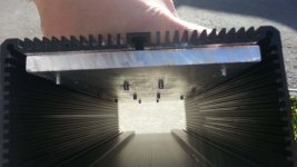
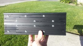
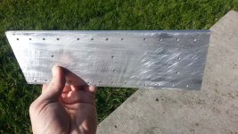
So I finally tried my hand at doing some "machining". I'm not good when it comes to working with metal so this is a bit challenging for me, but I'm learning. 2 days ago I didn't even know how to use a blocking and clamping kit. Today I finished up my heat sink plate, tapped it for 6-32 screws, milled some recesses in the case for screws and then drilled some holes for the screws to pass through. This is far from precision work, but my little mill let me do it better than if I had just done it all free hand. My precision will increase the more I use the machine. I really need to get a digital read out for it since counting turns and working the math for the 16 TPI screws is really annoying. I've had some issues with the indicators sticking on my horizontal axis which makes any kind of precision virtually impossible. It's still better than a regular drill press.

This case is much prettier than the other one, much smaller too. More pics to come as I continue this build.

I'm going to need some shorter screws to prevent them form protruding through the heat sink and possibly shorting to the exposed buss bars. I tried to setup the screw pattern to give me a even clamping force. I thought the middle might need some extra help to go flat against the case so I doubled up on either side of the channel, I goofed on the spacing to make it symmetrical though, oops. At least it's functional.

View attachment 6

case02.jpg

case03.jpg

View attachment 3

case05.jpg

case06.jpg

case07.jpg
 
The buss bar and capacitor setup. Wire connections will be made directly to the buss plates / bars, haven't decided exactly where the power feed will be yet. My heavy duty soldering is mostly done except for the wire connections. The big irons get heavy while working, but they work wonders since they were designed for stained glass work. With the 350W iron I can float an entire buss bar, but the real trick is setting up a fixture and avoiding the boards warping due to the elongation of the copper when it's hot.

As you can see flux clean up still needs to be done.

buss01.jpg

View attachment 6

View attachment 5

buss04.jpg

buss05.jpg

buss06.jpg

caps01.jpg

caps02.jpg
 
That's a crazy good work !

I love the design and controller case :wink: Hammond case are excellent for diy !

Just asking:

I wonder if you tought to re-melt the solder of the T--247 after you had bolted them to the aluminum plate?.

i'm asking because i see you soldered all these before and then yyou have bolted them... The legs are short and not very flexible so i think that the hight and paralelism of all To-247 might vary a bit and when you bolt them this might stress them a bit when one is not 100% aligned with the rest..

If you melt the solder o fthe legs a second time when the bolt are installed this will release the stress to all fets not perfectly aligned... and ensure that all fets will make the best mecanical contact because they are parallel and have all the same exact distance to the aluminum plate.
 
Thanks for the compliment Doctorbass, by my machine work isn't very good since this was only my 2nd time using my mini mill and I wasn't trying for precision or accuracy very hard, just wanted to "get it done". I'm not very good at working with metal, in fact I'd say I'm very poor at it, but now I'm learning. Would have been nicer to have a buddy do it, but I don't have a buddy that does machining now that I moved to California.

MOSFETs were soldered after being attached to the aluminum plate to prevent stressing, it acted as a jig. The MOSFETs align perfectly and lay as flat as possible against the board (they have 1 1210 size 0.5 ohm resistor under neath, the body almost touches), even if I rotate the board 180 degrees to mount it the wrong way on the heat sink. There is a even gap between the 0.25" plate and the bars, enough to make me not have to worry about them shorting out.

The tricky part was removing the warp on those long copper bars after they cooled. Takes a monster iron (I think the one I used weighs > 1kg, it's huge, but not my biggest) and some patience reworking it in sections, but after de-stressing the bars they are flat and so are the boards, it worked out really well. Should be ready to go for high current if the design proves to be decent. Under the MOSFETs are some SMD resistors to help stop gate - gate oscilations.

I didn't originally intend to fully cover the copper bars in solder, but figured it was a good move to stop surface oxidation and make a smooth solder transitions from the MOSFET legs easier. If I were to produce something this would require a redesign, but as a one off unit it's not too bad.
 
Been a few weeks since the last update. I had time to finish up the driver boards and get them mounted. I sanded down the areas on the heat sink where the FETs mount to get rid of the marks from filing for improved contact.

The driver boards are securely mounted, double 8 gauge wiring for the buss and single 8 for the phase output. Phase wiring is on the small side for any kind of serious continuous use, but for some high power short bursts it should be OK.

When you are making something like this by hand, there are a lot of man hours involved.
It's probably going to be a little while until I get to test it under power. I need to finish up designing my smaller Lebowski controller boards that fit inside this case. The design is almost done.

Enjoy the pics
View attachment 4

TO-247-18FET02.jpg

TO-247-18FET03.jpg

View attachment 1

 
Wow, that is the power board!

I built mine with a similar arrangement, horizontally placed IRFP4568-s, copper bars soldered on the PCB, and the FETs mounted on an Al bar, but it is a 12 FETs one.
My copper bars are not bars in fact, they are the same shape as the copper layers on the PCB, made of 1mm copper plate, and I cut them with dremel in several hours of work... :)

Did you consider using SMD ceramic capacitors instead of film caps?
Maybe more of them is needed, but they are smaller and then the board is more flat, and you could place the driver-controller board(s) parallel and close to the power board.
I used 10uF 100V ceramics, 2 in series for >100V, and one of this pack at each pair of FETs. This is 30uF altogether (6x5uF). I soldered the caps on 6 small pieces of PCB-s, and the terminals are soldered directly on the FET pins on the top side, between the drain of the upper and the source of the lower FET.

Unfortunetaly I don't have a photo and the board is in the bike, but this is my layout (the ceramic caps are not seen, because they are on the small PCB-s).
I tried to design is as compact as possible, the board size is 175x80mm (light blue lines). IR21844 drivers are placed on the power board, and J1..J7 connectors are going to the controller board. The controller board is smaller, and it is mounted above the FET area, on the right of the large electrolytic caps.

file.php


file.php
 

Attachments

  • top1.PNG
    246 KB · Views: 8,719
  • bottom1.PNG
    175.5 KB · Views: 8,718
good use of vertical gate driver to achieve higher power density. as long as the loop area is small, its totally fine. length of signal is not too important, even 6" is tolerable at high power levels.
 
peters said:
Wow, that is the power board!

I built mine with a similar arrangement, horizontally placed IRFP4568-s, copper bars soldered on the PCB, and the FETs mounted on an Al bar, but it is a 12 FETs one.
My copper bars are not bars in fact, they are the same shape as the copper layers on the PCB, made of 1mm copper plate, and I cut them with dremel in several hours of work... :)

Did you consider using SMD ceramic capacitors instead of film caps?
Maybe more of them is needed, but they are smaller and then the board is more flat, and you could place the driver-controller board(s) parallel and close to the power board.
I used 10uF 100V ceramics, 2 in series for >100V, and one of this pack at each pair of FETs. This is 30uF altogether (6x5uF). I soldered the caps on 6 small pieces of PCB-s, and the terminals are soldered directly on the FET pins on the top side, between the drain of the upper and the source of the lower FET.

Unfortunetaly I don't have a photo and the board is in the bike, but this is my layout (the ceramic caps are not seen, because they are on the small PCB-s).
I tried to design is as compact as possible, the board size is 175x80mm (light blue lines). IR21844 drivers are placed on the power board, and J1..J7 connectors are going to the controller board. The controller board is smaller, and it is mounted above the FET area, on the right of the large electrolytic caps.

Unfortunately I don't have much time to look at your layout, but several issues stand out. For high power you MUST use a laminated power buss. You do not want your gate drivers to cross over any of the power pass, your gate drivers are all sitting on the B- buss and have signals crossing into the power pass section, this is not good. Snubber capacitors should be rated for high di/dt use, they are typically classified as pulse rated. You only need one per phase bridging your buss as close to the high side drain and low side source as possible. 1-4uF is a typical value. Not sure what J4 and J2 do, but if those traces are carrying any kind of digital signal, you do not wan them crossing any power sections.

You might want to download and look at both of the gate driver and power layouts that I have posted on here. They are free for anyone to use. The one I used for Lebowskis controller has almost every component documented.

When you go high power, layout is critical. I just check the IR21844 datasheet and it does not appear to have any fault protection such as desaturation or a miller clamp. I would want a miller clamp at the minimum. Actually I probably won't design without desaturation detection now because it's saved me from blowing up dozens of MOSFETs during testing.

For a first design, size should not be a major concern, that is why my first controller is big an ugly, but works.

HighHopes has made many comments on design, it would be worth while to search his user name and read his posts. There are so many rules to learn in designing this work, took me a year to get where I'm at now and I started with a layout similar to yours.
 
Back
Top