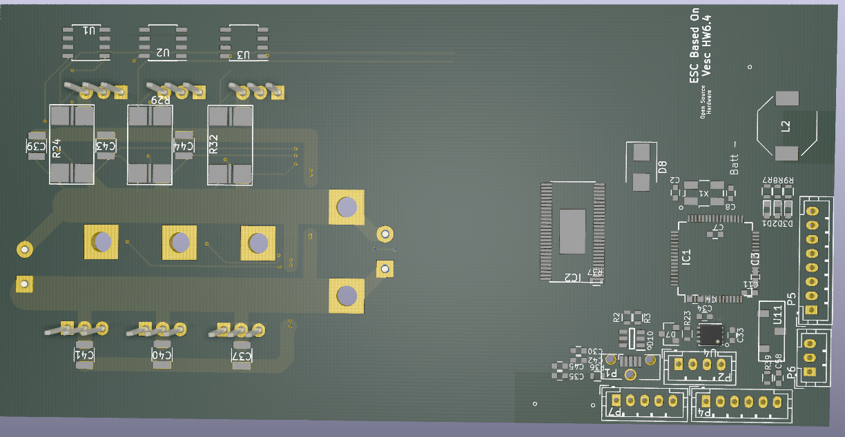
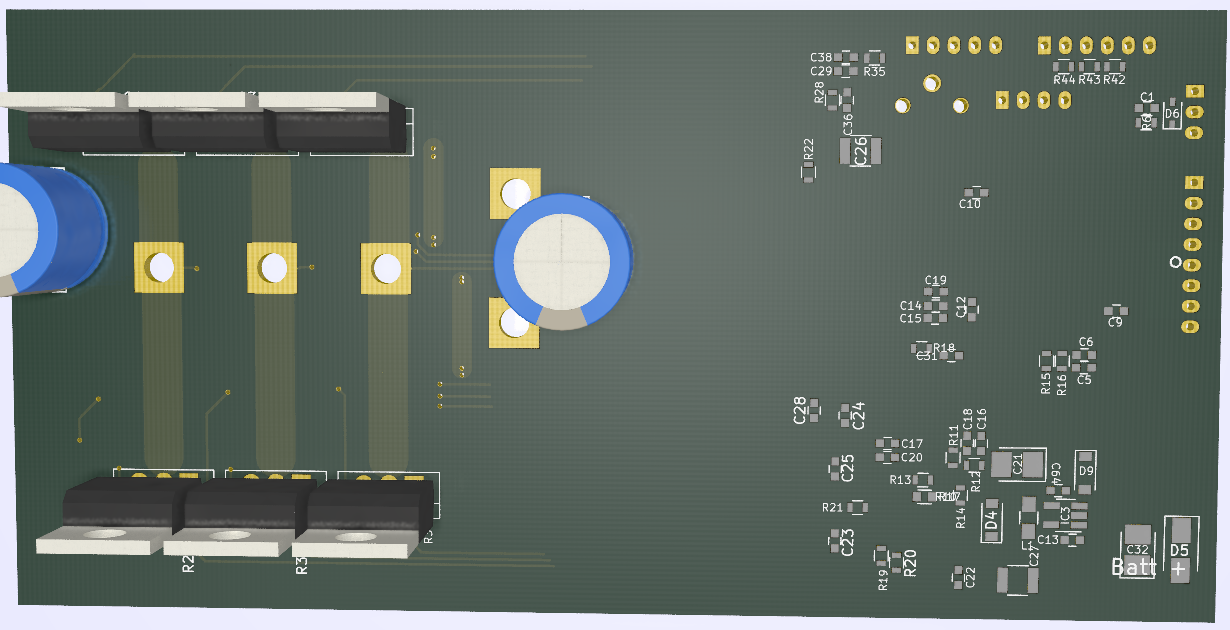
I grabbed a VESC 6 schematic from a thread somewhere and tried routing the power portion of it with TO220 FETs with the power rail layout I drew above and I think if you did end up using it or something similar you would easily be able to fit a 12 FET design into a 6 FET size aluminium extrusion box (125x35), even with the extra sensing components used on each phase. Inductance also wouldn't be worse, as you would keep the power entry location the same, but have your other 6 FETs on the other side (ie near the logic stage). It may be harder to avoid induced voltage spikes on your signal lines though.
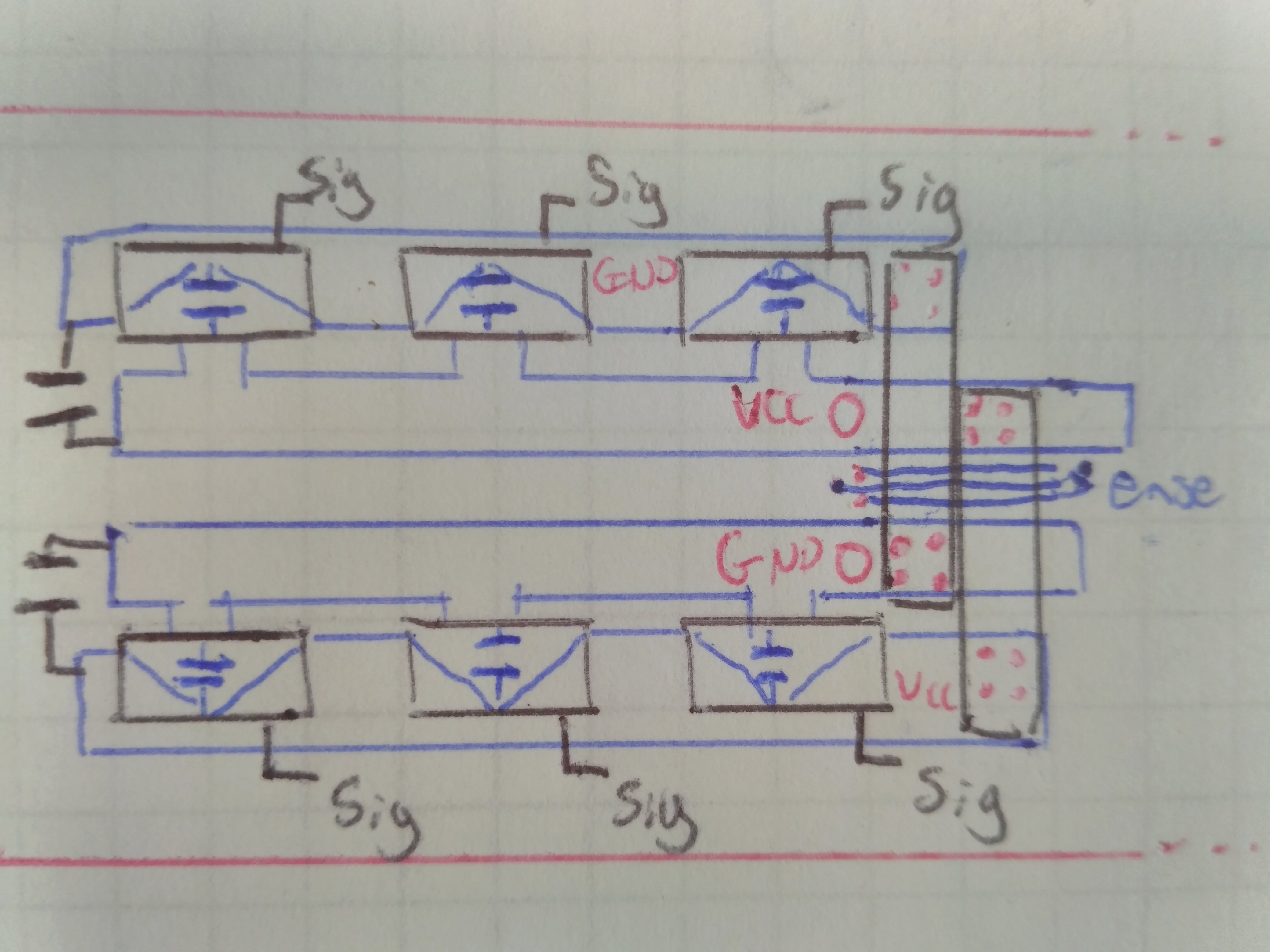
I could NOT however work out any way to have FETs at the top and bottom while having the power rails on opposing sides of the board from one another, without going to > 2 board layers, or having awful power routing. It would be possible with some stacked GND VCC laminated bus bars but that wouldn't really be in the realm of $30 cheap we are talking about.
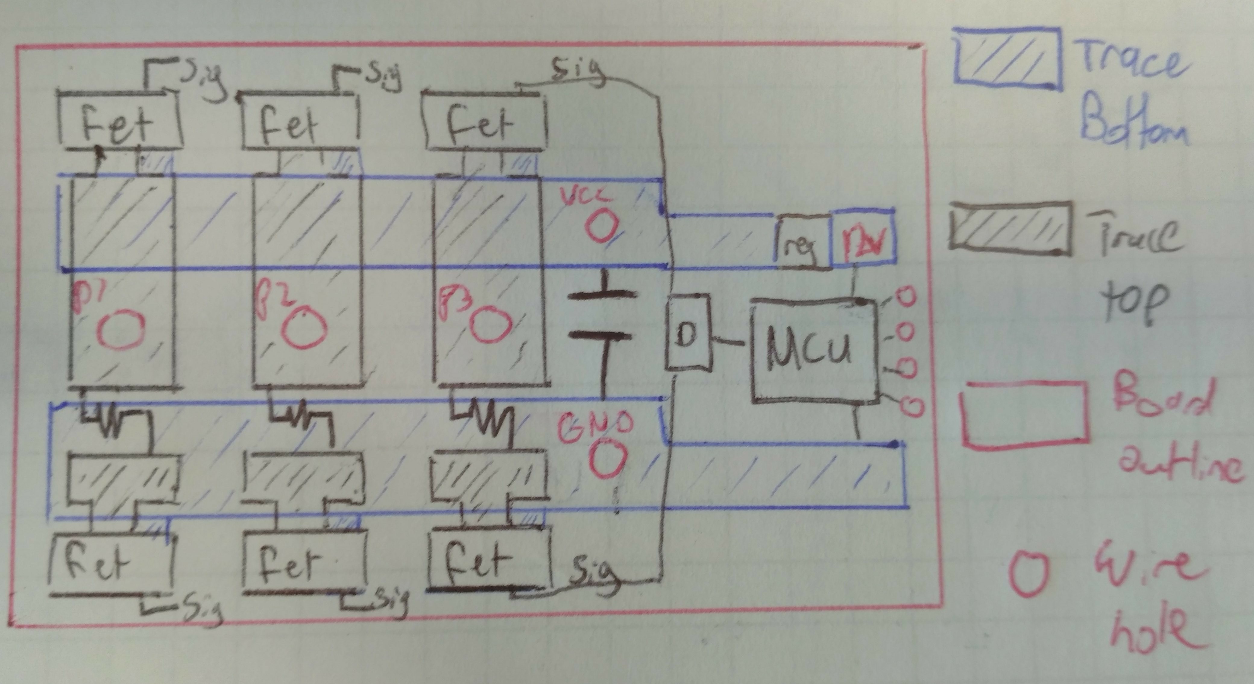
Excuse some strangeness to it, it's my first time in KiCad, normally I'm in Eagle. I couldn't work out how to do a copper fill area, I could only get it on the silkscreen layer, so the busses are just thick traces... and it's a KiCad v4 schematic imported to v5 so it's missing like half the package 3d models... anyway you can get the general idea from it.
You would also need a lot more capacitance to the power lines. You could get the power rails as close as your phase wire thickness if you eliminated the phase pad on the side of the board the rails run. This is kinda similar to
https://endless-sphere.com/forums/viewtopic.php?f=30&t=55641, but on a PCB instead so you have the thin side of the bus bar, vs the thick side close to one another.
nieles said:
it definitely WILL matter. any inductance between the bulk capacity and mosfet will cause voltage spikes and kill mosfets like crazy if you switch fast. and you want to switch as fast as you can to lower your switching losses. i have seen voltage spikes on a bad layout as high as 100v with a 30v supply.
I know you need capacitors as close to the FETs as possible to eliminate voltage spikes as much as possible from inductance (Which is huge on ebikes due to our long battery power cables.) I think in a top/bottom design you will be able to get both a large capacitor quite close to the FETs, and a smaller one right on the legs of it. I've got SMD caps in this design right on the legs, but you could definitely do a larger film cap instead. The low side caps are slightly further as they have to be after the current sensors > GND.
shaman said:
"Reduce the distance between the high side and low side IGBTs (I think this would apply to FETs too) to reduce the AC loop
inductance and to prevent damage to gate driver ICs."
I didn't realise that the board inductance was treated separately vs the inductance of the motor and phase wires. I was under the impression that since our motor and wiring had such large inductances, the most you could really do is limit your on board resistance. Now actually thinking about it as 3 separate inductors I can see how it matters. Still I think with a design like this your inductance wouldn't be particularly worse vs side by side FETs. You can also add thickness since we aren't using surface mounted directFETs.


.jpg")
.jpg")

