Yet another BMS

dmwahl said:
friendly1uk said:
Apart from an lcd display, my $25 board does all this.
Which board is that?

Smart bms sold by bmsbattery. Perhaps the best thing they sell. Though the pc interface is quite a bite at $100 more, if you need one. I think it's been hacked though if you see little point owning the real thing. You would need to read it's thread http://endless-sphere.com/forums/viewtopic.php?f=14&t=48461&hilit=oz890
 
friendly1uk said:
dmwahl said:
friendly1uk said:
Apart from an lcd display, my $25 board does all this.
Which board is that?

Smart bms sold by bmsbattery. Perhaps the best thing they sell. Though the pc interface is quite a bite at $100 more, if you need one. I think it's been hacked though if you see little point owning the real thing. You would need to read it's thread http://endless-sphere.com/forums/viewtopic.php?f=14&t=48461&hilit=oz890
Got it, I thought you had made your own.
 
dear friendly1uk, what are you talking about? I'm asking because it looks like you are talking about "smart bms" board, which is available for $20 from bmsbattery, yet you are stating in your signature that they are running funny business. Also I had that board and it is not so great as you make it look like.
 
Your right, and I knew saying it. I shouldn't put work their way. Them boards are outstanding though. I'm sure shortly after development the project would find it's way on to it's own board. Cutting out bmsb and the little niggles associated with them. It could be a fast moving project though.
 
Hi all,
To make it short, i've lost my smartbms account. So, fpie = smartbms.
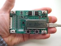
A new picture to proove my new identity.
DSCF3929small.JPG

I apologize for this late comeback. Some change in my life...
Saw that some people were interesting in that project. Please recontact me by PM. I'll answer.
DSCF4135.JPG

PS : I'll answer for some resonable request. Please do not ask me to make a 110S/300A BMS for your electric rocket.
 
Now interesting things for some potential interested guy (girls are also welcome :) )

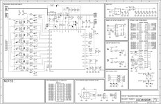
Schematic of this BMS :
FPIE_8S_BMS_REVA.jpg

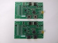
Some already reflow board (in a prototyping T-962A prototyping oven) :
DSCF4136.JPG

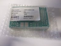
My stock of boards (more than a dozen from a batch of 20) :
DSCF4138.JPG

I give up soldering SMD components IC with hot air soldering station and other modified pizza oven in an uncontrolled way.
All this highly degrade components reliability, which sometime leads the component to burn when powered.
When this happend on a BMS, you can imagine what can be the consequences : fire !
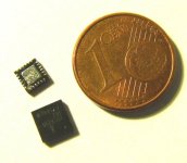
So prototyping oven what a real answer in term of reliability of my circuits, especially for ISL94203 which a 0.4mm pitch QFN.

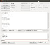
About software, the vital minimum is done. With a PC and an terminal, you can read/write each register of ISL, read out cells voltages, print LCD messages, etc.
8S_BMS_cutecom.jpg
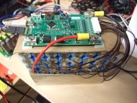
I declare 8 cells into ISL94203 (write FF at register 49) and read all the cells. Hum this brand "new" pack (make of an old stock of 2S4P samsung cells) really need to be balanced !

All this was made under Linux, Chibios is running into the STM32L. I wrote on year ago that firmware wasn't my cup of tea. But in fact, it's like the bike, i was just a little bit rusty.
I also come back into qt for another project, maybe i'll write something more sexy with gauges, bushbuttons, etc, rather than command lines.

By the way, why this sudden disclose ? One of the reason is because it tried to buy some more ISL94203, seeking ebay for some, i found my old post at the forth rank ! Whaouh.
The dark side of this is that I fear ISL94203 is close to be discontinued by Intersil, even if it is for me the best front-end for up to 8 cells BMS. It's the market law.

I'll post later the complete BOM of this board, with all needed components.

Hope this will be enough to revive some interrest...
 
Today i phone an Intersil FAE :
ISL94203 platform is, according to him, a big commercial success. So much that production have difficulties to follow the demand.
Thats why every distributor have empty stocks. So you can order some chips everywhere (mouser, digikey, future) but lead time is (and will) be at lead 12 weeks.
According to him (european market), two ebike's battery design is already based on this chipset...

FPie
 
circuit said:
This looks like a nice chip, and nice BMS.
Have you considered stacking several of these chips for at least 16s battery? Looks quite difficult to stack.

This chip is featured to be stacked once for an up to 16S BMS. It can manage two I2C adresses and have some extra pins to simplify i2c bus insulation and disable protection circuitry for the lower one (VDS of the two big MOSFET have to be adapted). I think that the upper block will consume slightly more during charge/discharge than lower one because of mosfet charge pump. Cell balancing will compensate that.

Some seens to have done this.
http://www.cebike.com/enterprise/qy0/gqxx.asp?id=118575&cpid=27359
lower ISL94203 seens to have overheat a little :)

I've discussed this with Intersil FAE, no reference design exist for this.
 
you should avoid bringing B+ back onto the BMS without having fused protection of anything over a few hundred mA. too much risk of very bad things happening if the B+ shorts to anything on the BMS.
 
dnmun said:
you should avoid bringing B+ back onto the BMS without having fused protection of anything over a few hundred mA. too much risk of very bad things happening if the B+ shorts to anything on the BMS.

I'm not so bad with an arc welder...
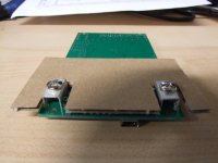
It's a moke-up, and this first release of PCB is for evaluation. But your remark have sense. I imagine mounting big screwed terminals on the "solder" side to separate wiring from electronics for some harsh environment testing. Then, terminal can pass through the wall of an insulating enclosure.

DSCF4145.JPG
 
I post schematics of this BMS, but what it's cost ?

Close to 30 euros (close to the same in dollar) of components without PCB. You can have a look to the BOM and associated cost at unit price and with my two favorite distributors : RS and Mouser.
View attachment 8S_BMS_bom.xls

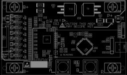
Here the placement of the board (size is 100x60mm) :
8S_BMS_placement.jpg

Note : I give these informations without any warranty. I do some software development and hardware validations, some things can change...
 
I am still dreaming about stacking these, so was looking around schematics. Source of T8 (discharge fet) is connected to output. So, if two of these chips are stacked, some pins of upper chip will be driven 2x below it's power supply.
Is it compatible with such voltage swings?
 
dmwahl said:
How warm do those big FETs get at 30A?
I've not tested yet mosfet temperature at 30A because my dynamic load can't sink more than 150W (50V/15A) and i'm not at stage of validations (i'm developing firmware, coulomb counting at this time).
What i usually do is is a testing board equipped with "special" mosfets and shunt with worse value than real, that allow me to "qualify" behaviour of my design at only a fraction of the full power and do some temperature measurements to deduct Rth of my design.

With the actual NXP PSMN1R7-60 mosfet (2milliohms) , at 30A i roughly dissipate 30x30x0.002 ohms so 1.8 Watts per mosfet and 30x30x0.001 ohms into 0.9W into shunts.
Total of 2 mosfets + shunts, less than 5W, less than 1% if your consider a 8S battery at 30A.

Notice that ISL94203 have two NTC input. One is dedicated to monitor mosfets temperature, it's a feature of ISL94203.
 
you do not need battery voltage on the BMS. it is a fuse in the negative lead. do not bring the B+ output to the BMS which is at ground.

if you need power to run the BMS from the top of the pack then use a lead that is fused at the B+ terminal to allow no more then the 100mA you need to run your electronics. same with the charging lead, use a fused lead from the B+ terminal to the + lead from your charger.

this is an indication of poor design and is always a fail on the chinese low quality BMS. you do not want your design to be tainted by the same poor practice.
 
fpie said:
dmwahl said:
How warm do those big FETs get at 30A?
I've not tested yet mosfet temperature at 30A because my dynamic load can't sink more than 150W (50V/15A) and i'm not at stage of validations (i'm developing firmware, coulomb counting at this time).
What i usually do is is a testing board equipped with "special" mosfets and shunt with worse value than real, that allow me to "qualify" behaviour of my design at only a fraction of the full power and do some temperature measurements to deduct Rth of my design.

With the actual NXP PSMN1R7-60 mosfet (2milliohms) , at 30A i roughly dissipate 30x30x0.002 ohms so 1.8 Watts per mosfet and 30x30x0.001 ohms into 0.9W into shunts.
Total of 2 mosfets + shunts, less than 5W, less than 1% if your consider a 8S battery at 30A.

Notice that ISL94203 have two NTC input. One is dedicated to monitor mosfets temperature, it's a feature of ISL94203.
I doubt you'll have any issues at that power level, I was mostly just curious. I spent the first 5 or so years of my career doing thermal management for single board computers, and it's amazing how many people just look at the datasheet Rth and go with that, not realizing it's totally unrealistic for most designs. Glad to see you're doing it the proper way and actually measuring temp :)
 
dnmun said:
you do not need battery voltage on the BMS. it is a fuse in the negative lead. do not bring the B+ output to the BMS which is at ground.

if you need power to run the BMS from the top of the pack then use a lead that is fused at the B+ terminal to allow no more then the 100mA you need to run your electronics. same with the charging lead, use a fused lead from the B+ terminal to the + lead from your charger.

this is an indication of poor design and is always a fail on the chinese low quality BMS. you do not want your design to be tainted by the same poor practice.
I agree with you on the fusing, but are you concerned about a failure of the ISL part or casual shorts due to something touching B+? There are plenty of points on the board with enough potential to cause damage if shorted. I've not dealt with a lot of the chinese BMSes so I'm not too familiar with what they're doing.
 
circuit said:
I am still dreaming about stacking these, so was looking around schematics. Source of T8 (discharge fet) is connected to output. So, if two of these chips are stacked, some pins of upper chip will be driven 2x below it's power supply.
Is it compatible with such voltage swings?

In my case i use 60V VDS mosfets, just OK for 8S design (i like have some margin). For a 16S design, the 2nd ISL94203 should be 100V rated. If you have a look to datasheet, you'll see a Rdson and charge of gate increasing dramatically.
On the other hand, i'm not shure than ISL94203 built-in gate driver will turn off bigg 100V MOSFET (maybe 2 in parrallel to keep the 30A capacity) soon enough to do it's short-circuit protection role (electronic fuse role). ISL will "open mosfet" slowly because of big gate charging. A fuse in that case is a better solution. You can keep the charge mosfet protection (lower current i guess), but i would not bet a penny on the CC protection feature.

Such design, even if features exist in ISL94203 for (separated SDAI/SDAO pins to insulate I2C, CASC bit of 0x4A register) have no reference design according Intersil FAE. I can understand that electric community would like to have something more than 8S to make their electric vehicule go faster. For me, 8S just fit my needs. It's a challenge for hobbyist to go on this solution. You'll need a big stock of spare...
 
the major fires i have seen with lifepo4 packs was due to the charging lead running though the BMS housing. the risk is in the large currents that can flow on the main positive conductor if it is shorted to the source legs of the output mosfets so there is no way to stop the current and that leads to the overheating and fire.

i see it often on the very cheapest BMSs because they find it cheaper to leave off the one top sense wire so they bring B+ back to the BMS and use it for the top of the pack sense wire. they do the same with the B0 sense wire and use the B- or ground lead as the B0 sense wire. both cases add the current induced deltaV to the sense wire detection voltage.

fusing that lead helps and it doesn't need to be a large conductor to carry enuff current to run your circuit.
 
dnmun said:
the major fires i have seen with lifepo4 packs was due to the charging lead running though the BMS housing. the risk is in the large currents that can flow on the main positive conductor if it is shorted to the source legs of the output mosfets so there is no way to stop the current and that leads to the overheating and fire.

i see it often on the very cheapest BMSs because they find it cheaper to leave off the one top sense wire so they bring B+ back to the BMS and use it for the top of the pack sense wire. they do the same with the B0 sense wire and use the B- or ground lead as the B0 sense wire. both cases add the current induced deltaV to the sense wire detection voltage.

fusing that lead helps and it doesn't need to be a large conductor to carry enuff current to run your circuit.

Okay, maybe the next release of PCB.
I actually concentrate all my efforts on firmware.
 
Back
Top