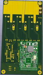
Power PCB for Lebowski Controller to be combined with Bobc's processor board

Lebowski said:
I hear your comments... Swapping the place of the gate drivers and current sensors:

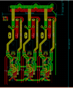
pic1.png
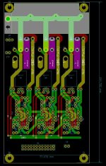
pic3.png
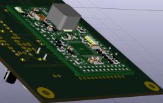
pic2-800x800.png

I like the straight shot of the output to the current sensors. If I only use the top layer for the high current path, then I can route the gate signals underneath the current sensors.

What I don't really like is the long gate driver wires. An online inductance calculator tells me that the inductance fo two flat 2mm wires spaced at 2.54mm is 16nH per cm (so 160nH for 10 cm). The Ciss of the Fets is 7 nF (for ITXH180) or 20nF (for 4468's). The turn-off gate resistor is between 4.7 and 10 Ohm.

Damping is 0.5 * R * sqrt(C/L).

So the 4468 with 4.7 Ohm gives a damping of 0.83
The ITXH180 with 10 Ohm gives a damping of 1.05

Both numbers do not impress me, I would like to have had 2 or higher... the cause is of course the high wiring L.

P.S. no clue why some pictures show up bigger than others... even when I make all 800 pixels wide they still show up differently ?
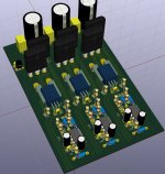
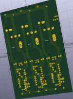
I agree the long gate drivers are bad hence my suggestion that you move the gate drivers to where you currently have the snubber/link caps and move caps to between the fets and the new current sensor location.
 
Think I've got it now:
pic1-modified.jpg
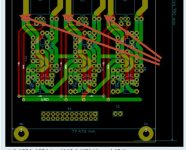
pic2.png
pic3.png

The 'clou' it that the gate drive lines are no longer 2mm track spaced 2.54mm (with a 16nH/cm inductance) but now are 3mm wide track opposite each other on both layers of the PCB (giving a 6.7nH/cm inductance).
This reduced inductance can be used to space the gate drivers further away, making room for the current sensors.

The output of the FETs it now a straight shot on the top metal to the current sensor. The output can be taken at the other side of the current sensors, either top or bottom of the PCB. Regarding the bottom, the hole at the current sensor terminal is now 1.6mm (same as FETs), but maybe 2.5 or 3 mm should be better...
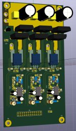
 
By default you get 1.6mm thick pcbs, you can order a thinner pcb, like 1mm thick which will easily lower the inductance. 1mm is still pretty rigid. At 0.8mm you get some flex which may or may not affect you, depends on components weight but mostly in pcb mounting points.
 
Another thing to keep in mind with PCBs is when fattening up the tracks or adding extra copper wires... they can warp when they get heated up during soldering. I will get the standard 1.6mm for my test pcb...
 
Lebowski said:
Think I've got it now:
pic1-modified.jpg
pic2.png
pic3.png

The 'clou' it that the gate drive lines are no longer 2mm track spaced 2.54mm (with a 16nH/cm inductance) but now are 3mm wide track opposite each other on both layers of the PCB (giving a 6.7nH/cm inductance).
This reduced inductance can be used to space the gate drivers further away, making room for the current sensors.

The output of the FETs it now a straight shot on the top metal to the current sensor. The output can be taken at the other side of the current sensors, either top or bottom of the PCB. Regarding the bottom, the hole at the current sensor terminal is now 1.6mm (same as FETs), but maybe 2.5 or 3 mm should be better...

Nice job, I vote 3mm for the phase wire output from the current sensors.
 
This looks really clean, logical and easy to solder. Piece of art! And still <80mm wide ;)
Brainboard hovering over the drivers I assume?
 
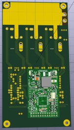
front with the busbar and high current wiring exposed for soldering

pic1-1024x1024.jpg

processor board piggybacking on the main board. Note the exposed battery line to the drain of the high side FETs, this line is exactly on the other side of the PCB as the ground to the low side source, continuing the busbar idea.
With the way the 3.2 mm holes are for the battery and motor phase wires they can be connected either to top or bottom of the PCB.

The way I see it, the PCB is mounted upside down in a box with the cooling connected to the box. Underneath the lid you have the 5 high current wires, and easy access to the processor board with its setup/reset switch and its RS232, throttle and hall connectors.

pic2-1024x1024.jpg

Note: in the 24 pin connector both the processor board and the PCB have one square pin (all others are round), the square pins must line up.

pic3-1024x1024.jpg

Note how processor ground (so 5V ground) is taken from the central FETs, this point will be kind of star connected (though much won't remain of the star when I fill the bottom part with a ground plane.

pic4-1024x1024.jpg

With the bus bars filled in you can also see how the low side gate drive (same as high side by the way) is connected with Kelvin contacts.
 
2 quick notes, one silly, one not.

* looks like the current sensor footprint lacks the large thrugh hole pads.
* Can you guys add a mounting point to the control board? if its only supported by a header you're looking for troubles, you want a screw in there, at least one like m.2. Especially with wiring coming out of that pcb.
 
Not a bad plan. I was thinking regarding securing the brainboard to the power board I would design and print custom plastic spacers for the other end to the header. If there is a hole in the middle there Bas, it would make it very secure and easy to fasten the board securely down. Good shout Marcos.

potential mounting hole points.jpg

i reckon you have some space here to put the holes to allow for the plastic spacer.
 
great work lebowski. if i didn't already have one of your fantastic controllers, i would build one immediately.
i hope that this project leads to many new user for your controller!
btw i just found a great source for pcbs: https://jlcpcb.com/ they are super cheap, especially for prototypes.
 
Just a thought when I see this nice development, sorry for the distraction... It looks like lebowski's original through hole board (without drivers and current sensors) could be shrinked to the same size as this power board. Wouldn't it be nice to have the option if Bobc's tiny SMD processor board could be fitted to the power board or a redesigned lebowski through hole board? Both via the same 24 pin connector?
 
not sure i understand here Emgee, Bobc brain board is the brain and the two dcdc convertors, so when you look at lebowskis original through hole board and take those two things away, all you are left with is the drivers and the current sensors.

When you think about it, Lebowski is putting both the drivers, the current sensors and the mosfets on the "power board".

I think maybe you are asking if you could had an alternative to the bobc smd brain that hooks to this powerboard. There maybe a point in having a through hole board (with only the pic and the dcdc's) so you can plug that in but you will be making it all bigger again.

I think once we are really producing the smd boards efficiently, it wont make sense to go back to the old soic pic and through hole dcdc.
 
Yes, that's the point: The option (for DIY soldering amateurs) to combine the through hole power board with a through hole brain board (mainly the PIC and 2x DC/DC) via the same connector as for the bobc brain. So the through hole philosophy would be consistent.
I agree that a nice SMD brain board is 'better' in many ways (probably I will buy one myself when available). But then a (small) SMD power board would be the consistent 'partner'. If we could agree on a common connector and it's placement on the boards, everything would be interchangable. Good for flexibility, repairs etc.
Don't get me wrong: I like the actual status a lot and don't want to distract, just thinking...
 
10cm is not an issue for gate drive as long as it is over the proper ground plane (not possible on current design). Another possible compromise is to use twisted pair for your gate drive and eliminate the traces all together. The twisted pair will be much less likely to experience ringing. It also has the added benefit of being able to setup proper high/low ground planes at the gate driver as well. What you have now will most likely work ok due to being lowish power.
 
How does twisted pair compare to shielded cable (like mini coax) ???

I have been thinking about my Micro-Lebowski and could just solve all these issues if I used short pigtail leads instead of PCB traces...

Thanks
Andy
 
Basic simplified theory:

Shielded cable just shields against external signals inducing into the center conductor(s) by sending them to ground.

Twisted pair has currents flowing thru closely-paired conductors equally, so cancelling out induced noise.


Practice can be a little different, depending on actual conditions.
 
But you don't need shielding against interference in the 15V low impedance gate drive. What you need is low jnductance to prevent ringing, and for this twisting the gate drive wires works,

But the goal of this PCB is to have everything on the board without needing to handwire the gate drive of 6 fets. I think many people are put of the other PCB because of the need to hand wire the power stage. This power pcb for bobcs processor board has all connections on the pcb, so no need for hand wiring. It only need some fattening up of the high current traces as the PCB copper is too thin.
 
Ok good to know... I was under the impression that noise / interference would be a problem as well.

So conceptually, If I keep the gate signal closely coupled with its reference (either GND for low side and phase-out for high side) by having the reference immediately below, and possibly beside as well? It should be right... Yes?

Thanks
Andy
 
Animalector said:
Ok good to know... I was under the impression that noise / interference would be a problem as well.

So conceptually, If I keep the gate signal closely coupled with its reference (either GND for low side and phase-out for high side) by having the reference immediately below, and possibly beside as well? It should be right... Yes?

Thanks
Andy
What you need is low inductance wiring between gate driver chip and FETs. I used this online inductance calculator to get an idea of the inductance per cm for side-by-side wiring and one-on-top-of-the-other wiring:
https://www.eeweb.com/tools/broadside-trace-inductance

Based on this I concluded that side-by-side gives too much inductance (and a risk of ringing due to low damping, see the calculations a few posts back). But the one-on-top-of-the-other gives much lower inductance,and much less risk of ringing, so this is the option I chose.
 
all wired up and DRC clean :D

pic1-1024x1024.jpg

I added ground planes in the bottom half around the processor board connector, but not around the gate drivers. This to keep the low inductance traces intact, and to keep the star connection I have at the bottom part of the board.

I moved the power stage caps up a bit towards the edge, to have more room for working with the soldering iron, and for more room to fatten up the PCB bus bars.

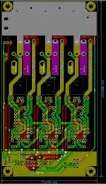
pic2-1024x1024.jpg

note the second temp sensor in the bottom left... this is a place holder for a connector to wire up multiple temp sensors (maybe for in the motor ?)

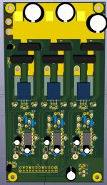
pic3-1024x1024.jpg

the wiring is so tight, where to put 2.5 mm holes for more rigidly mounting the processor board ?
 
Back
Top