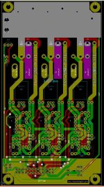
Power PCB for Lebowski Controller to be combined with Bobc's processor board

Lebowski said:
Thats the one position I tried, gave DRC error..
Thats why you first define your assembly and mounting points and then you do layout :mrgreen: . I wish I could help you there.

Don't you need through holes on the big terminals of the current sensors? Looks like you exposed the copper to use both layer as current carrying.

Remember that your control board connector is on the top layer and your actual control board is on bottom side. Maybe there is a chance you have that connector mirrored, I've seen that happen.
 
You pull the tracks a little to the left, even just making them make half roundabout, making space for the holes.
 
If you move the tracks and make yourself some mounting holes, we could use some 3d printed PCB clips that holds the edges of the CPU board. And then a touch of silicon to hold it.

I can model some clips of you give me the board spacing, PCB thickness and hole size.
Andy
 
Lebowski said:
Thats the one position I tried, gave DRC error..

Just the presence of the holes? Or only with a screw in situ?

If the latter, perhaps those click-fit plastic standoff would work:
DSCN2738.JPG


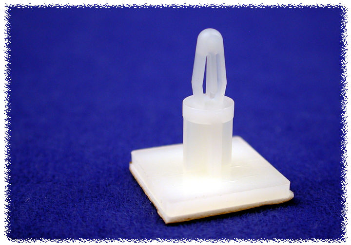
If the former, maybe self-adhesive standoffs would suffice:
PCB2_B.jpg
 
These could save the day. Saved mine back in the day.

https://www.digikey.com/product-detail/en/keystone-electronics/9018/36-9018-ND/2746023

It constrains you to 1.6mm thick pcb though.
 
I was thinking exactly like that with press pins for the bottom (power board) but then the top (CPU board) would have edge clips that hold onto the sides of the PCB. Because there are no holes in the CPU board..
 
Solderable "dummy pins" (from 2.54mm male-male SIL headers) to conserve PCB space?
 
minimum said:
Solderable "dummy pins" (from 2.54mm male-male SIL headers) to conserve PCB space?

Looks like a good idea until you need to take out the board for some rework or repair...
 
I added 2.5 mm holes:
pic4-1024x1024.jpg
As already mentioned in the 3rd post of this thread, I see the need for mounting holes for a support for the processor board. But to sacrifice electrical performance, however minute, for some mounting holes ... hurts my engineering soul :?

Anyway, I had to route one line to the other side via 2 vias.. But I want to have all vias easy to solder through, maybe even with a small bit of wire. Don't really trust the manufacturers vias that much, plus some people may want to make their own boards at home. So the solder mask will be removed around all vias exposing the copper, and the hole will be relatively large for a via (0.8mm) to allow insertion of a bit of wire.
 
1 question/suggestion : it seems to me that we can pile-up 2 or 3 of this power board to make it a 12/18 FET controller. Apart from shorting the current censors on additional boards and keep them on 1 board only, what other modifications might be needed ?
 
Better to have one brain and a bigger control board. Perhaps in the future Lebowski will extend on this design for higher power levels
 
kawak said:
1 question/suggestion : it seems to me that we can pile-up 2 or 3 of this power board to make it a 12/18 FET controller. Apart from shorting the current censors on additional boards and keep them on 1 board only, what other modifications might be needed ?

Bit risky but worth a try. I think all it needs is resistors at the current sensor outputs such that the feedback voltage provided to the processor board is the average of the current sensor outputs. This way you can have 150 A sensors on each board, but for 2 or 3 boards in parallel the effective current sensor would be 300 or 450 A respectively. I would run a bit longer deadtime than absolute minimum to account for switching delays (runtime differences) between the different power boards.
 
Glad that kawak was bringing it up. I like the piling-up idea following lebowski's "low inductance output stage construction" thread.
If three fully equipped Power PCB's would be stacked with their outputs from the current sensors in parallel (with common GND): Wouldn't the controller just 'see' the average voltage of the current sensors? No modifications needed, just split the battery and phase wires?
 
P1 silkscreen on the wrong side

P3 and P5 are probably connected to chassis. There is exposed copper like 1mm away with battery voltage.

Do those external dimensions fit nicely in an enclosure? extruded for example. I see no clearance on the edges to slide it into an extruded enclosure.

board ID? version? mfg date?

Its mostly random stuff that one might want, but forgets.
 
Some good points there, thanks Marcos.

- I'm only putting the component outline in the silkscreen, not their designation (gets real messy real quick)
- reduced the copper circle around the 4 corner mounting holes
- On request from emmgee I've kept the width below 80 mm (it's at 78 now), so to add empty space for sliding... His bike will hopefully be the test vehicle for this build. Plus I'm only getting 5 boards and will post the Kicad data base in the first post of this thread, so everyone can make the changes they want
- added a date to the board ('jan 2018')
 
By coincidence I was just checking the dimensions of a Lyen-type controller and a BMS this morning... both have a similar sliding case with inner dimensions of ~ 72 x 140 x 32 mm. With 78 x 145 mm at the moment we are very close, but a further reduction of a few mm in each dimension seems difficult. For the testing of the first boards it's maybe better to leave it as it is (works well for me!). Of course the future optimisation for a cheap chinese controller case would be nice, maybe (if waterproof) suited to be attached to the front tube.
What disturbs me... this mounting hole really hurts a bit... nowadays they attach loudspeakers with velcro to walls... ;)
 
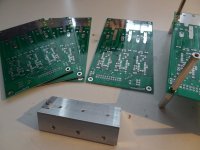
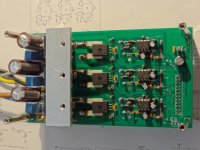
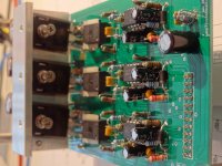
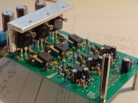
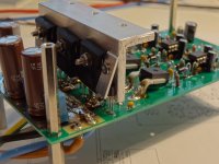
So the boards showed up :D

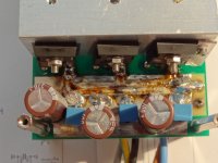
Made an aluminium piece to attach to the main heatsink, with an additional little screw for clamping the temp sensor
DSC02026-800x800.jpg

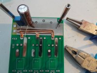
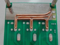
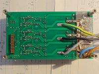
Fatting up traces with copper wire
DSC02027-800x800.jpg
DSC02028-800x800.jpg

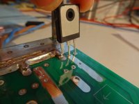
A piece needs to be cut off the low side FETs source, as theres no hole for this leg:
DSC02037-800x800.jpg

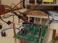
First test setup for determining the gate resistors for the 4468 (note also the added insulation pads to the heatsink to prevent shorts):
DSC02048-800x800.jpg
 
I've added a table to the first post giving recommendations for R_on, R_off and deadtime for different FET types.

I also added all scope pictures of the measurements, for reference.
 
I've not soldered any headers to the boards yet but I notice yours are male headers from the power stage.

1) I don't know If I have female headers in a 12x2
2) I cant work out from your PCB which pins are which so I will no know which side to solder a header to even if I had one
(I will leave that to you I think), should make it flater to post.

btw I've been very Ill with tonsillitis but I am making some progress.
 
Back
Top