VESC based +200A powerstage with 200V MOSFETs (videos of it in action)

zombiess said:
.The VESC software is only measuring the inductance at 1/3rd of actual on my meter. I need to look at the code and try some different motors. Maybe I can mod the code to be more accurate for the PI controller gain calcs.

Inductance measurement error is a known vesc issue on 3rd party hardware. I guess it works better the faster the powerstage switches, and at lower f_sw I get more accurate results. Shaman was also concerned about this, and many people would be interested on fixing this issue.
 
benjamin posted a reply to shaman's questions/observations about the inductance measurement error on the VESC forum a few months ago - https://www.vesc-project.com/comment/5097
 
marcos said:
Inductance measurement error is a known vesc issue on 3rd party hardware. I guess it works better the faster the powerstage switches, and at lower f_sw I get more accurate results. Shaman was also concerned about this, and many people would be interested on fixing this issue.

I'm still a total noob when it comes to VESC and am learning as I go. Shaman and I have been talking quite a bit and he's mentioned the issues he's experienced with switching speeds. I ran my setup at <100ns D-S switching speeds and then at 300ns and the results on motor detection and FOC control have been identical, however I am unable to place any significant load on my motors right now as I don't have a proper load cell. I'm building a desktop load cell this weekend. The only load cell I do have is 45kg and is in my garage, not exactly the best indoor unit.

bww129 said:
benjamin posted a reply to shaman's questions/observations about the inductance measurement error on the VESC forum a few months ago - https://www.vesc-project.com/comment/5097

Thank you for that link. This VESC is a lot of searching around to figure out what does what. It would be nice if there were some documentation.

BTW, you should make an electric drive for the < 18yr old Yonies to put on their buggies. It always cracked me up when I heard a buggie with a sound system in it bumping some NWA (90s) as the horse went clip clop clip clop. (I grew up in the Lancaster/Berks area). When murdered out cars became a thing on the west coast I thought everyone just went Mennonite. Schwarza bumpa.
 
zombiess said:
BTW, you should make an electric drive for the < 18yr old Yonies to put on their buggies. It always cracked me up when I heard a buggie with a sound system in it bumping some NWA (90s) as the horse went clip clop clip clop. (I grew up in the Lancaster/Berks area). When murdered out cars became a thing on the west coast I thought everyone just went Mennonite. Schwarza bumpa.

The Amish are much less progressive than most Mennonites who have adopted more aspects of modern society. You won't ever hear a real Amish buggy with a sound system. :lol: That's pretty hilarious you grew up in the Lancaster area. Not a lot of people know about, let alone have seen, the phenomena that you describe but it is very real. I still remember the first time I saw a horse and buggy as a kid when my family moved here back in the 90s. They're still very common to see on the roads, especially in the southern end of Lancaster. A couple of geared hub motors on a buggy wouldn't be a bad thing to help out the horses when they have to pull a whole family up the hill!
 
[youtube]LcJCTB-6k2c[/youtube]

I setup a large out runner motor, a 120100 70KV motor with 9uH inductance. I do a bit of a walk through and scope shots during the video. Sorry it's shaky, I need to get a stabilizer and do better planning if I'm going to do this type of video. This was done off the cuff with no planning, just me talking about what I'm doing. I like to make videos during some of my lab work as they can make good notes when I need to review something.
 
I finally found a dyno that can take the power. Dual ME-0913. I shorted out the phase leads on the load motor, so at this point the controller is pretty much running into a locked rotor scenario at 200A phase. This is the worst case scenario for a controller. These motors are 15uH and 6.8mOhm. If I disconnect one set of windings I get 33uH/14mOhm. Now that I've done the locked rotor testing that is what I'll probably do.

Tonights testing verified that hardware over current detection works as well as desat. This PCB only has a sum 2.5oz copper for the high current paths, I was able to determine that the controller can run 65-70A. I put 200A phase through it and from 25C it got to 80C in about 30s. Final boards should be 4-6oz copper per layer, so a minimum of 8oz vs the current 2.5oz.

MOSFET temps were never able to exceed 45C unless the heat sink was not installed.

No issues running without a resolver. Sensorless FOC is keeping track of the rotor position without issues and zero difficult starts.
 

Attachments

  • Dyno-ME0913.jpg
    Dyno-ME0913.jpg
    189 KB · Views: 2,569
  • Dyno-ME0913-Drive.jpg
    Dyno-ME0913-Drive.jpg
    202.2 KB · Views: 2,569
  • Dyno-ME0913-shorted.jpg
    Dyno-ME0913-shorted.jpg
    181.2 KB · Views: 2,569
  • Controller-4awg.jpg
    Controller-4awg.jpg
    230.6 KB · Views: 2,568
Damn, this is nice stuff.. I was working on a separated control and power stage controller but now I feel I missed out on picking your brain for a lot of stuff.

Your control board looks nice. Is it open source? I would like to see the schematics if possible. Looks like you have optos on all your IO lines.

I'm new to VESC so I just wanted to throw something basic on a PCB and give things a play and learn a bit about how to interface VESC software with hardware.

What types of changes did you find you needed to make to the VESC software to interact with your control and drive boards?

I totally forgot about all the cool stuff you were building when I was last on this forum ages ago.

I'm still running a Lyen controller at 125v 30S with IRFB4115. Ahh the good ole days eh? When power was just enough.


Mo
 
Hey mystamo,

I haven't made this current design open source. I'm not sure if I'm going to take this down that road or not. It might be worth while to get more people interested in my higher power designs I have in progress (+1000A).

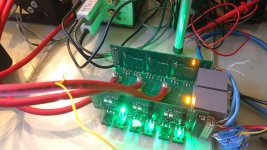
My VESC controller is similar to the Axiom schematic, but I've modified it quite a bit to suit my own needs and reduce cost. There isn't anything unique about it's design, it's just several standard practices combined. I did not isolate my phase and DC bus voltage measurements with ISOamps like Axiom did because everything is running through voltage dividers. The chance of high voltage making it across the divider is pretty small, at 200V there is only 5mA available after the first part of the voltage divider which consists of three 13k resistors in series. If the low side resistor were to fail, then it's possible this 200V @ 5mA could find it's way onto the controller, where it runs into a op amp which is used to convert the 0-5V signal into a 0-3.3V signal for the Adc input of the processor. The risk for injury is low. Lethal current starts > 100mA from everything I've read so far. An end user would also have to complete the circuit to ground while touching the high votlage.

All other signals from the power stage are isolated, current sensors and gate driver which includes fault detection and PWM.

All voltage and current signals are fed into an active Butterworth low pass filter for noise reduction. I decided to keep all my sensor interfaces at 5V vs 3.3V to increase the signal to noise ratio. All the digital inputs to the processor are processed through by directional 5V-3.3V converters.

As for getting the VESC to run, I had to build out a Linux environment for compiling the firmware and verify I could successfully build the stock VESC firmware on GIT. After that it was a matter of plodding through the .h and .c files in the hwconf directory. I made several side by side comparisons with the Axiom conf files as they are using external sensors. It was a matter of hacking and slashing my way through the code for about 3 days, then finding several errors I had made in wiring up my controller. Messing up wiring on the first go is almost a given, it was just minor stuff like swapping phase A and C signals. Because I have hardware fault detection I wasn't overly concerned about causing damage. The error codes on my LED readout really clued me into what my issues where, I was getting shoot through, but it doesn't damage anything as the current is shut down by the gate drive in about 5us.

I'll need to do a 2nd revision of my controller boards to fix the minor errors it has, but I'm contemplating offering up this as a VESC controller to the community as a finished product which is independent of the power stage with an public schematic so end users can tweak options like filter frequency.

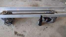
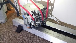
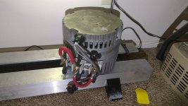
I'm going to be looking for others to test out a complete controller, but I'll probably need some commitments from interested parties before going into production. The power stage will be enclosed in a 3D printed case for protection, and I'm contemplating adding forced air cooling to the MOSFETs and PCBs to further increase the potential for abusive power levels. :twisted:

I've added the shunts to my current sensors and they now read to 400A, however I'm unable to get over 220A because my DC bus voltage drops. This is probably a limitation of my 30V 100A power supply and it's long power leads. I'm planning to build a battery pack for more testing. I think I have 30 5Ah 6s LiPo packs. They are old and have double the internal resistance vs when they were new, but they appear to still hold a charge well enough. I just need to plan it out so it's safe to use, last thing I want is a battery fire.

I'm going to get some video of the controller pushing ~200A and time how long it takes to get to 80C on the PCB and MOSFETs
 
[youtube]rn65suIcXQ0 [/youtube]

I upgraded the dyno and set it to torture mode.
180A phase current into a very high load. The FOC algorithm help up fine.
 
Zombiess, You are so epic good man. Thanks for the really in depth explanation.

I can see already my controller is a bit of a joke in comparison to yours. But I'm coming off the old lyen controller days still have that on my ebike running irfb4115's at 30s 50a. Been doing that for YEARS with no problem. So I feel vesc and these new gate drivers are such leaps and bounds ahead I should still be ok with my controller design even tho it lacks all the error proofing yours has. Fets are also so much more capable these days.

What does your fault detection circuit look like? Mine currently looks like holding the fault pin on the mcu high via a pull up. LOL!

Mo
 
mystamo said:
What does your fault detection circuit look like? Mine currently looks like holding the fault pin on the mcu high via a pull up. LOL!

That's the same method I use when I generate a fault, pull the MCU pin low. I have added an additional layer of hardware fault detection which operates by pulling the enable pin high on a transceiver chip which the PWM passes through. The fault signal is output through a bunch of 74HC series logic after comparators filter the current and voltage signals through a butterworth filter. It's similar to Axiom, but not as robust. I went with discreet logic because I don't have the time to learn FPGA skills. Downside is the space the discrete logic board takes up, but it's low cost.

I'm trying to keep costs down so if I'm able to produce a product on this I can keep it affordable. I can up the quality from where I'm at now, but it ups the costs so I aimed for lower specs.
 
Very nice work, zombiess. Glad to see you back in the game with the VESC option.
I've been working on my high voltage VESC design for the last three years and I am pretty close to a full scale production.
I went through multiple iterations with early ones using TO-247s but ended up with TO-Leadless mosfets on a single layer Al substrate to kill two birds with one stone: reduce parasitic inductance and provide direct heat dissipation interface via the board to the heatsink. Additionally, this makes the power stage compact and easy to assemble.

https://endless-sphere.com/forums/viewtopic.php?f=31&t=99621
 
Powervelocity.com said:
I went through multiple iterations with early ones using TO-247s but ended up with TO-Leadless mosfets on a single layer Al substrate to kill two birds with one stone: reduce parasitic inductance and provide direct heat dissipation interface via the board to the heatsink.

I've never had much love for SMD power devices. How much parasitic inductance does the power pass section have?
 
Powervelocity.com said:
I haven't gotten to measuring the inductance on the boards but signals look good under load.
SMD power parts on FR4 would likely be a bad idea, but it works great so far on Aluminum substrate.

Yeah, SMD on FR4 doesn't seem like a good idea. My curiosity is in the loop area created by using a single sided PCB as it prevents the generated fields from overlapping as much as a layered design and less cancellation. Are you carrying any current through the metal substrate? I had looked into doing something like this but decided not to due to assembly issues.

I'd be interested in seeing a double pulse turn on/off into a +200a pulse.

You can measure the inductance by looking at the turn off ringing frequency, then add a 100nF cap (or something else > 47nF) across drain-source of a MOSFET and fire the pulse again and see what the frequency is. From there it's just some math to figure out the parasitic inductance/capacitance of the DC bus.

I've posted a link to how to do it previously somewhere. I have a spreadsheet I created so I just enter the frequencies and added capacitance.

*edit* I found the app note that shows you how to measure it.
https://assets.nexperia.com/documents/application-note/AN11160.pdf

If you want to PM me your ring frequency before adding a cap, then add the 100nF cap and tell me the frequency again, I can tell you how much the LC parasitics are. I'm very curious to see how well the layout performs as there are some nice SMD devices. I've had some plans to use them, but I need to make carriers for them.
 
Thanks for the note on the double pulse test. I attempted to pulse from within VESC firmware at some point but it didn't work at that time, so I just went on testing under load and monitoring the gate signals and the DC link. I am also using 3x 10mf PP Film caps on top of about 3F worth of electrolytics. I do have placeholder for snubbers just in case I ever need to use them. I have one controller running on a bike up to 300A phase and 106v voltage max.

My half-bridge layout looks like shown below. You are right that it's hard to keep the loop to the minimum on a single layer but I think it's worth the trouble for a very good thermal interface that Al substrate provides. My drivers are on the DC link board which is 4 layers, so all the gate routing is done deferentially there. The power stage board has 4oz copper but I also add copper strips to beef up the current handling. In my tests, I deliberately restrict airflow around the controller. It stays under 50C most of the time even in this California heat.

half_bridge.PNG
 
Powervelocity.com said:
Thanks for the note on the double pulse test. I attempted to pulse from within VESC firmware at some point but it didn't work at that time, so I just went on testing under load and monitoring the gate signals and the DC link.

Making measurements on a running motor generally produces non repeatable results and can lead to incorrect conclusions. You might want to program up an Arduino based pulse circuit so you can perform repeatable tests. Your load can just be a coil of wire, I use a wire spool with about 25uH inductance. You only need to do this on a half bridge.

I am also using 3x 10mf PP Film caps on top of about 3F worth of electrolytics. I do have placeholder for snubbers just in case I ever need to use them. I have one controller running on a bike up to 300A phase and 106v voltage max.

3x 10mF? I think you mean uF. 10mF = 10,000uF. 3F of electrolytics is 3,000,000uF. I think you might be off by 3 orders of magnitude on both those :wink:

My half-bridge layout looks like shown below. You are right that it's hard to keep the loop to the minimum on a single layer but I think it's worth the trouble for a very good thermal interface that Al substrate provides.

I'd be very cautious about the way you have routed that gate trace. A rule of gate driver design is that no part of the gate trace should enter the power pass section (flying leads can somewhat skate this if properly routed 90 degrees to the magnetic field and kept far enough away). In lower power designs it's also possible to get by with crossing the power pass at a 90 degree angle to the flux field, but still not good practice.

In your design, the gate trace is surrounded by the power pass and is in the middle of the loop area, and in parallel with it, pretty much a worst case scenario. This could lead to an induced voltage on the gate trace which causes miller effect turn on and lead to the MOSFET being partially on in the transconductance zone where it generates a lot of heat, or worse, full turn on leading to a shoot through event. I don't know what gate driver you are using, but if you are moving forward with this design I encourage you to use a gate driver with a miller clamp. I would also use a negative gate bias voltage of at least -5V when off to reduce the chances of accidental turn on and verify nothing is questionable under repeatable lab conditions. Issues like these are one of the reasons I've stayed away from SMD devices. I've tried many layouts, but I couldn't make it happen without breaking the design rules I learned. You are into a current level where miller effect can rear its ugly head, I've been surprised how much of it I've seen even on my own designs where the gate driver has used a miller clamp. The effect may be reduced by slowing the switching time of the MOSFETs as it's induction is tied to dI/dt.
 
mFd, uF, µF. I guess I am old school. mF is something I saw written on my dad's boxes with electronic components decades ago, so mF just stuck with me. Sorry for the confusion.

I know that my approach is non-orthodox and I meant it to do it differently this time. Is it ideal? No. Is there a room for improvement. Yes, of course. This is a work in progress and it will get better over time.

I do slow down switching and I am using faster turnoff to mitigate the switching losses. Additionally, there are fast acting over voltage and over current circuits to minimize the possibility of a catastrophic event in case something goes wrong.

With that said, I am continuously investigating opportunities to improve the design and I appreciate the advice.

zombiess said:
I'd be very cautious about the way you have routed that gate trace. A rule of gate driver design is that no part of the gate trace should enter the power pass section (flying leads can somewhat skate this if properly routed 90 degrees to the magnetic field and kept far enough away). In lower power designs it's also possible to get by with crossing the power pass at a 90 degree angle to the flux field, but still not good practice.

In your design, the gate trace is surrounded by the power pass and is in the middle of the loop area, and in parallel with it, pretty much a worst case scenario. This could lead to an induced voltage on the gate trace which causes miller effect turn on and lead to the MOSFET being partially on in the transconductance zone where it generates a lot of heat, or worse, full turn on leading to a shoot through event. I don't know what gate driver you are using, but if you are moving forward with this design I encourage you to use a gate driver with a miller clamp. I would also use a negative gate bias voltage of at least -5V when off to reduce the chances of accidental turn on and verify nothing is questionable under repeatable lab conditions. Issues like these are one of the reasons I've stayed away from SMD devices. I've tried many layouts, but I couldn't make it happen without breaking the design rules I learned. You are into a current level where miller effect can rear its ugly head, I've been surprised how much of it I've seen even on my own designs where the gate driver has used a miller clamp. The effect may be reduced by slowing the switching time of the MOSFETs as it's induction is tied to dI/dt.
 
with respect to IMS power stages I found PCBWay was letting you specify a 2 layer, 3oz (105μm) per layer, IMS PCB for not wildly more than a single layer. By putting both layers on the top side of the aluminium you'd get approximately 100μm spacing between the copper making for a low inductance bus bar. It would also be possible to run the gate traces very close to their corresponding source traces to tighten the current loop. You'd still have to deal with the aluminium ~100μm from the lower plane however.

I was getting <$300 for x10 2L 3oz 2mm Alu IMS on their calculator.
 
The last time I checked, 2 layer IBS boards were expensive enough to not worth the trouble. This may be changing quickly though.
One issue is that copper is often limited to 3-4 oz max and that's not enough to support the desired power ratings. For my purpose, 1 layer + copper strips work well so far, but pending more testing.

As for the DC link board is made of FR 4 layers, with the power tracks properly sandwiched to create laminated bus bar and the gate routes are routed deferentially in adjacent layers.

Apart from that, all the control circuit is completely isolated from the power stage. Even halls and motor temperature go through isolators.


Pinski1 said:
with respect to IMS power stages I found PCBWay was letting you specify a 2 layer, 3oz (105μm) per layer, IMS PCB for not wildly more than a single layer. By putting both layers on the top side of the aluminium you'd get approximately 100μm spacing between the copper making for a low inductance bus bar. It would also be possible to run the gate traces very close to their corresponding source traces to tighten the current loop. You'd still have to deal with the aluminium ~100μm from the lower plane however.

I was getting <$300 for x10 2L 3oz 2mm Alu IMS on their calculator.
 
One of the advantages of IMS is you get to double the effective copper thickness, so 3oz IMS is equivalent to 6oz FR4. One big advantage of that is you don't have to worry about larger track & gap allowances that higher copper thicknesses push you towards.

You're always going to have to run some low voltage/current signals on the power stage assembly, gate drive, phase sense, even current sensors assuming you want fast resistor/op-amp based ones.

It's definitely a changing landscape and there does seem to be a slow trend towards brushless and compact high power inverters.
 
That's true. IMS has lower requirements for the copper weight, you can run approx. 2x more current compared to equal weight copper on FR4. I run 4oz, but also solder 1x5mm copper strip alone the power tracks to be sure there is enough ampacity for at least 500A. Where IMS+SMD power switches really shine is that the power stage can be mostly machine assembled and reflowed. Hand assembling works fine for a few prototypes but when I need to make hundreds of these, that's where it really scales up well.
I agree any design will have tradeoffs geared towards the target application.

By the way, speaking about fault detection, I've just tested the my HW overvoltange and overcurrent circuit made of a few cheap comparators. Seems like it's working well triggering at overcurrent at least at about 400A according to graphs but I am thinking graphs may not be capturing the actual spike because I set it to trigger at 550A. I am also using ACS current sensors with bypass shunts for a effective resolution of 2.1mv/A. Someone was warning about non-linearity with bypass shunts but so far, it has worked well up to 400A. I am yet to test above that.

Pinski1 said:
One of the advantages of IMS is you get to double the effective copper thickness, so 3oz IMS is equivalent to 6oz FR4. One big advantage of that is you don't have to worry about larger track & gap allowances that higher copper thicknesses push you towards.

You're always going to have to run some low voltage/current signals on the power stage assembly, gate drive, phase sense, even current sensors assuming you want fast resistor/op-amp based ones.

It's definitely a changing landscape and there does seem to be a slow trend towards brushless and compact high power inverters.
 
zombiess said:
The silicone pad really surprised me, I did not expect it to perform as well as the tape due to how much thicker it is.

I've been thinking about this on and off and after a little digging, found a thermal conductivity figure for Kapton of .12W/m*K. Inexpensive thermal pad I've seen around has a conductivity of 1-2W/mK. Based on these numbers, a .5-1mm thick piece of ordinary silicon thermal pad has the same conductivity as a 2-4 mil (.05 - .1 mm) sheet of Kapton, ignoring other advantages like conforming to the surface in question. Not so surprising in that context.
 
SRFirefox said:
I've been thinking about this on and off and after a little digging, found a thermal conductivity figure for Kapton of .12W/m*K. Inexpensive thermal pad I've seen around has a conductivity of 1-2W/mK. Based on these numbers, a .5-1mm thick piece of ordinary silicon thermal pad has the same conductivity as a 2-4 mil (.05 - .1 mm) sheet of Kapton, ignoring other advantages like conforming to the surface in question. Not so surprising in that context.

Thanks for digging up that info, it's useful to know. I knew Kapton wasn't the greatest, but I wasn't expecting it to be an order of magnitude worse at that thickness.
 
Back
Top