Spot Welding Copper Strips to 18650 Battery Cells

Laser cutting thin metal sheet can be cheap and lots of places do it. - machine cost might typically be 30 an hour. Pretty standard for steel fabrication shops. Recommend you do a DXF for them to make their life easy (recommend "Fusion 360" free software)
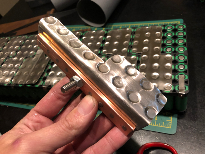
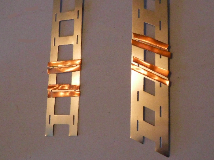
Copper to nickel - silly question but why not solder or braze the nickel to the copper - no super powered welding needed.

So, tongue in cheek, in theory:
£20 cash - for laser cutting, £20 solder and blowtorch - nickel strip to copper, £20 ebay welder with bigger wires to weld to cells another £20 for couple of car batteries from scrap yard and £20 for a normal battery charger A bit redneck but should work and all for £/$100.

Battery vs other power - lead acid has no problem with short bursts of high current (lithium probably less tolerant) if you use 2000A for 20 mS every 10S then a bog standard battery charger with an average currant of 4A will do. Cheaper than ultracaps. Tricky to get ultracaps to do 2000A for a budget according to spec though they might work...

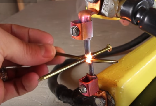
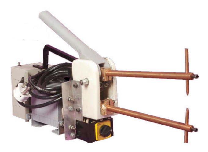
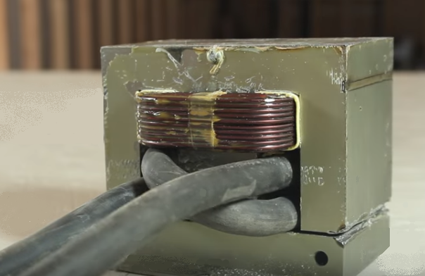
Hmmm - 68,000 welds - yeah, maybe some tungsten tips for those electrodes. Don't think you'll need to drop to 0.1 nickel with a K-weld though or need more than 1200A if 0.15 is all you're doing, I do 0.15 + pure nickel using a car battery that struggles to start my car & a slightly modified £20 welder - 10% of the cost of a K-weld but havent done thousands. Reckon I could get to 2000A with better batteries and 3000 with better cables, probes and a freewheeling diode. Not sure what the 2000A limiting factor is that you mention for the Kweld - the FETs look as though they'd take a lot more. Resistance in the whole system is the challenge for mine . If you double the capacity of the supply you don't get double the current unless you also halve the resistance of everything else in the circuit.

Ref overall resistance I'd recommend you do your resistors in parallel and series calcs for the whole circuit. A prototype - making a single pack and using a good resolution (10microvolt or better) meter with constant current supply through the circuit is pretty good for identifying areas of high resistance (set to 1A and 1 mV = 1v in 1000A use - scale as appropriate).

One test is worth a bunch of theory etc
 
The goal is a solid welded connection between the copper and the batteries.

Nickel just makes that possible with an inexpensive spot welder, the "DIY code" for doing copper directly hasn't been cracked yet.
 
That's exactly my thought: There are people who have managed to weld THIN copper to a battery cell BUT: my fear is whether I can do tens of thousands of welds without burning through a cell bottom. Or after 4 hours of continuous welding I get delirious and don't notice I'm running a bit hot and doing a partial melt through. How would I know? 38 cells in parallel per block, 112 blocks....

And I already figured I need a minimum of 1.5mm copper plate to carry the current, preferably 2.0mm, and there is no way to weld 2.0mm copper plate to a battery can.

So the nickel to battery connection seems the most foolproof, reliable way for me to do it. Welding the nickel to the copper plate should be doable since there will be no cells involved yet, I can focus on a nice hot deep weld there. So I weld the 0.15mm nickel plate to the 2.0mm perforated copper plate first. Then flip it over and weld THROUGH the holes in the copper plate so I'm welding 0.15mm nickel to the cell.

BTW the kWeld manual says that it has a hard current limit of 2000A programmed in as a safety limit. It also warns that the freewheeling diode can get overstressed with long output cables.

I thought about soldering or brazing the thin nickel plate to the copper plate but not sure how. How to keep the nickel plate flat as I heat it up, etc. Remember this plate is something like 4 x 12 inches. I'm sure it could be done, but not in my kitchen oven! So I'm thinking the spot welding process should work. It'll be a bit tedious, but I can use the same equipment (my soon-to-arrive kWelder). I'd love to hear any ideas on alternate ways to bond the nickel to the copper plate.

And yes, planning some immediate experiments when the welder arrives. I plan to just nibble some test holes in the copper sheet, spot weld the nickel plate over the hole and then weld to a single cell can. I can put 5A of current through it with my small lab supply and I have a voltmeter that will measure down to .0001 volt. That should let me map out the voltage drops pretty well without having to fabricate a final plate and weld up 38 cells. Thinking of checking the resistance with 2 pairs of welds from nickel to cell and then 2, 4, 6 and 8 welds from nickel to copper.
 
67carguy said:
So I weld the 0.15mm nickel plate to the 2.0mm perforated copper plate first. Then flip it over and weld THROUGH the holes in the copper plate so I'm welding 0.15mm nickel to the cell.

You are not going to be able to weld that with the KWeld. The copper sinks the heat too quickly. A WAG would be 15 kA to be able to make those welds.

I am just soldering my 0.2mm nickel to the 2mm copper plates.
 
BobBob said:
Laser cutting thin metal sheet can be cheap and lots of places do it. - machine cost might typically be 30 an hour. Pretty standard for steel fabrication shops. Recommend you do a DXF for them to make their life easy (recommend "Fusion 360" free software)

So I did that yesterday. Fusion 360 has to be the most un-intuitive software ever developed. It took me 4 hours to make 3 simple extruded 2d parts. The array function is maddeningly slow, as was the dxf export. I felt at those times like I was using the old 3D Cad software on my Atari ST.

I'm not sure if a shop would need the 2D extruded version with depth or just simple 2D.
 
Sorry you didn't get on with Fusion360 I thought it was pretty good for free. played with it a bit, I prefer solidworks but we have licences at work and I don't feel like shelling out for a home version of SolidW.
Happy to send you a DXF if you sketch what you want
2D DXF will be fine, no dims or writing needed just make sure you get the scale and units right. If you're the sort of person to wander in and chat about an interesting project, you may get a better cash price, particularly if you supply your own material, no tooling needed, just machine time and I expect work is sporadic at the moment.

General thinking around the problem, forgive the essay:
Running with the copper bus with nickel tabs (which is slightly off topic for the thread): If you had slightly wider strip or individual pieces slightly larger than the holes you could solder braze or weld round the edge of each - whichever method you prefer but it would take a longer than spot welding. for a manual process I'd say spot welding and ultrasonic are probably the only fast contenders. (US is not as far along the DIY route yet).
You could also weld tabs then mechanically bolt / clamp/ rivet etc to bus plate
Nickel and copper both solder or braze easily. The chances of the laminated result warping are higher if it's a solid sheet with a solid layer of braze so smaller bits may be better. Coefficient of thremal expansion for nickel is around10% greater than copper which is not much but... Electrical resistance may be better with solder (right to the edge and lots of X section) but thicker nickel will make more difference so as you're going for 0.1 I guess that's not an issue

If you're getting the copper lasered, you could also get the nickel lasered to whatever pattern you like, to optimise current through the cell (improve welds) rather than through the copper (difficult as you can't have infinite slit with a copper bus plate - IE the weld current will prefer going through your bus plate if it's designed well. I'm thinking a cross rather than a slit might be good to reduce flow. I'd say do the maths but it's a bit of a pain to work out so I'd make a few - might use this as an excuse to find a friendly laser place - say I'm trying out different shapes and put the whole lot into a single sheet. Might ask at work about automating the shape optimisation but don't hold your breath - that's getting a bit clever for software design.

Off track
er-guess it would be possible to laser to weld 2 mm copper to cans? The challenge (same as for us) is getting a load of heat into the weld in a short space of time to melt the metal locally without heating the surroundings - kit may be a bit pricey though and the control optics can be tricky (last one I had quoted was around £120K).

Further of track, yeah you could fit it in the oven
I've had cast iron doors in my mate's oven before TIGing it with stainless. I managed to build a plate heat exchanger in my kitchen once. My girlfreiend came home to myself and three work colleagues with a 600 x 800mm copper plate and around 5 metres of copper pipe on our 5 burner hob with all burners going, a blowtorch and a mapp gas torch and clouds of flux fumes filling the house- it rather depends on who you're sharing your living space with I'm still with her 18 years on.

2000A limit for safety - hmmm, none of this is shouting safety at me I have to admit.
I expect you could fool the software into thinking there was less currant and boost it a bit if you could be bothered
If the freewheeling diode is stressed I'd put another in parallel, keep the leads short etc. won't matter if you're using 0.1 - that will be fine at 1500A with the K weld, 0.3 pure nickel only on my rig struggles at 1600A and 100 mS which is too long, even with a slot so it wouldn't work with the copper bus plate design without going to 3000A or a wonderful system such as ridethelightening built

John
With conduction in 4 directions and the ability to weld thicker nickel than nickel and copper with the same kit it would be interesting to work out which would give better resistance. Nice thing about holey copper is ability to make the copper thicker so it improving series resistance without affecting per cell nickel tabs (Again, sorry, off topic essay)

Nickel plating- I think we still have the resisitors in parallel problem that 90% of the weld current will go through the copper rather than the cell which is mainly steel and so will not heat up because copper is a better conductor. Had a play this eve and with 0.3, the strip gets hot but nothing much goes through the cell
 
You are not going to be able to weld that with the KWeld. The copper sinks the heat too quickly. A WAG would be 15 kA to be able to make those welds

Hmmm... I was afraid it might be tough. I'm wondering if maybe I need a completely different setup to laminate the .15mm nickel to the 2mm copper. Actually, I've been so focused on the cell welding I'm forgetting this step does not involve the cells. Maybe I use more standard spot welding techniques. Maybe ground the copper plate, then go around with a single tungsten electrode tap a handful of welds around the holes in the copper plate. I'll need a template so I know I'm hitting over the copper and not the hole in the copper. Maybe a simple MOT (BIG MOT, or several) type welder with a timer is all it would take.

Make my 224 end plates with typical spotwelding techniques, then use the kWeld to finesse a nice weld from the 0.15mm nickel to the cell. That still might take some manly power because the copper plate will not be far away...

And I won't have to wait for my kWelder to come in!
 
If you've already ordered the kWeld, I would suggest that you simply try it out and see how it goes. You might be surprised. That being said, the 0.15mm copper and 0.15mm nickel have been welded with success onto 18650 cells with the kWeld, using the "copper/nickel sandwich" method...

Since copper is four times more conductive than nickel, then a 0.15mm copper bus would be the equivalent of 0.60mm nickel, with the added benefit of fewer watts being converted to waste-heat.
 
I have not tried thicker than 0.2mm copper so 2mm must be totaly different beast to weld. Maybe if electrodes are placed on opposite sides (one against 2mm copper and another 0.15mm nickel side) it would be easier or even possible to weld :roll:.
 
BobBob said:
Happy to send you a DXF if you sketch what you want
2D DXF will be fine, no dims or writing needed just make sure you get the scale and units right.

Thanks Bob. It worked, mainly the move/copy portion I found very tricky to get to work, along with the direction for the pattern (array). With enough YouTube videos I finally figured it out.

If you are interested, here is the file I finally wound up with. The target sheet is 24"x24" and this takes up most of it with a little space left on the sides and bottom. I elongated the holes to make it easier to spot weld across the split in the nickel since the current is running North/South between the two rows of cells.

20200919_busbar_sheet_layout.jpg
https://drive.google.com/file/d/1kg3eIFuVWwPpn9VokFpVRMQ552HqrQj9/view?usp=sharing
 
Always interested, thanks for posting pic
I believe the split in the nickel you mention is so that the weld power goes through the cell. - I'd need to see the nickel layer to confirm what you mean about elongation and know whether North / South is top right to bottom left or top left to bottom right :)
If there is a stonking great copper bus bar bridging the strips then split nickel may potentially not work as an approach?

To make it really difficult and complicated if you like that sort of thing: Make use of laser technology (cheap variability) and free software, try a load of different concepts and configurations to see which one is best
If you love the software, use shape optimisation in F360 (clever (read complicated) stuff). Tricky bit will be looking at the thermal propagation of the weld through multiple metals along with the temperature/resistance variation in a 3D multi material structure and optimising for that. Yeah, that's pretty advanced stuff but this is a use for it.

Theory
Basically you need resistance to weld but want to avoid resistance during use so need to vary the shape so the resistance directs the current to heat the welds to the battery during welding but conducts with minimal resistance when working.

Also forgot to say, recomend 0.000,01 V not 0.000,1 resolution - for looking for resistance - gets you to mm position which is useful I'm cheap and use a holdpeak HP-6205 for £22 (it doesn't meet it's own spec for low current DC Amps but is great for mS transients and higher currents for the price) cheap 6000 count meter.
 
Could someone please address the idea of simply plating the copper sheet/bus with nickel to facilitate using Kweld to do it all in one pass?

How thick does the nickel plating need to be to give enough resistance - thermal too, or just electric?
 
by spinningmagnets » Sep 19 2020 2:29pm

If you've already ordered the kWeld, I would suggest that you simply try it out and see how it goes. You might be surprised. That being said, the 0.15mm copper and 0.15mm nickel have been welded with success onto 18650 cells with the kWeld, using the "copper/nickel sandwich" method...

I saw that thread, and it was very interesting. I have a few concerns though. I have not tried it yet, I'll need my kWelder to come in first. But from what I understand, the nickel melts right through the copper to form a weld with the cell. I don't know if anyone has done any detailed analysis of the welds, but I'm curious if the copper sheet is actually part of the weld or if the copper material is simply pushed out of the way as the nickel melts it and welds to the cell can. I'm concerned that if there is no actual copper to nickel weld, then the joint could be subject to corrosion over time.

My second concern is that for my particular application (getting 1200 amps from the 38P cell block) to do a direct copper-to-cell weld may be out of the question. I'll need 2.0mm copper plate for a reasonable voltage drop. With copper that thick, I suspect I would never get consistent welds to the thin can without burning a hole in the cell can.

That's why I'm looking at using nickel to bridge a small gap from copper to the cell.
 
In the sandwich method, the copper melts onto the cell (you can Dremel across the center of a weld to see the cross-section). The cell end is nickel-plated steel, both have high resistance. When you place a probe on that material and send a pulse through it to something that is conductive on the other side, the pulse travels a fairly straight path, which would be the path of least resistance due to the resistance that is also radiating out to the sides of the probe contact through the nickel.

If you put a probe onto pure copper over a cell and pulse it, the copper is so conductive that the pulse spreads out and flows into the entire contact area of the cell. But when current flows through a nickel ribbon first, none of the current wants to flow around the nickel on the sides of the probe contact. In this way, the nickel strip acts like a lens that focuses the current into something similar to a laser.

If you set only copper sheet over a cell tip and hit it with a welding probe, its a like a garden hose nozzle set to shower-spray. If there is nickel above and below the copper, the top-nickel focuses the welding energy like a beam, because no energy wants to spread out through the nickel in a radiant direction.

Imagine we are using a large/wide bus strip of the common shape and there is a 16mm slot over the cell, and if you put a probe tip on each side of the slot, the probe tips are 8mm apart. Track the current during a weld. If the cell-tip is steel, and the bus is nickel, the current can travel 8mm to the end of the slot, make a U-turn, and travel 8mm to the other welding probe-tip (16mm ), or...it can go one millimeter down into the cell, 8mm over to the other side, and one millimeter up to the other probe (10mm). It takes the path of least resistance, which is the short path...and incidentally along the way it welds the pressure points. The flat bus material is touching the cell all around the probe tip, but due to flex in the bus material, only the Tiny area under the probe-tip down-pressure has the best conductivity / least resistance.

Then...consider a pure copper sheet as a bus material instead of having any nickel there. What has more resistance? an 8mm path down/over/and up through nickel...or passing sideways through 16mm of copper bus? This is why I included pics of the "infinite slot" bus-shape. Even with the added distance to travel, the copper path has the least resistance.
 
1200 amps from the 38P

You only need thick copper buses at the two pack ends, the positive and negative collectors. You are only drawing 31A per cell, so 0.20mm thick copper is all you need for the cell buses. Making those buses thicker will not help, and it would make welding more difficult.

If you were mapping the current, the copper bar shown could be thinner at the two ends, and thicker in the middle next to the connecting bolt.

BatteryBusBars2.png
 
Plating - thinking out loud, not hopeful - the heat generated via resistance is dependent on the thickness of resistant material. so as the voltage drop times the current provides the heat and there is low thickness, the voltage drop and heating effect will be minimal. Might be good as it's already stuck to the copper - nickel may stick to nickel better. won't corrode etc

Due to good mechanical bonding (the plating) with the copper, thermal transfer will be high so the thermal mass of the copper will prevent the plating getting very hot. If an infinite slot is not used or if there is a copper bus as per 67carguy's suggestion, the current will tend to flow through that

Copper nickel sandwich:
Not convinced by the "nickel acting as a lens" theory - my working hypothesis is thermal tranfer due to higher resistance causes the weld.
Even if the lens theory did work, the point source would be the same as for a probe tip being at that point on the copper.
For infinite slot, most of the heat will be generated by the nickel and steel, but we may need to put enough heat into the nickel for it to (probably) mainly melt the copper by conduction (test this by varying the thickness of the top layer of nickel without changing anything else), the specific heat capacity is similar for copper and nickel (10% greater for nickel) so with equal thicknesses of copper and nickel I'm guessing we need to double the power into the weld plus a bit for inefficiencies and losses of thermal conductivity which is 4x higher for copper so we lose a bit more but get the heat into the weld a bit faster. Melting point for copper is lower than Nickel so likely to melt and you can alloy nickel and copper so there's a good chance it will stick. I don't know the typical weld pool depth for a spot weld where it turns liquid or how much it is plastic (the pressure will tend to squeeze the liquid out and there will be some plastic deformation around the weld.

My crappy copper probes stick to nickel though not particularly well so I'd want to see some reliability data before relying on it

Without infinite slot, a simplistic guestimate would put around 250A going sideways through the nickel only during the weld, 1000A is likely to go sideways through the copper (1/4 of the resistance) and 450A through the 0.3mm steel can (worse resistance but double the thickness)

As copper is a great thermal and electrical conductor, the heat generated per volume of copper at a current is 1/4 so despite taking all the current, it will heat up less as each unit of heat is heating 4X the volume.
The heat generated to weld the cell to the copper may therefore mainly come from the steel can and may be only around 20% of the power.

Moving from simplistic to 3D, the cross section that the current flows through will be pretty small at the probe tip - combined with that fact that all the current goes through here means the top layer of nickel is likely to get much hotter than normal. conversely instead of a point contact from deforming the nickel strip onto a battery and the high level of heat at that point, we've spread it through an intermediate copper plate. I'd expect the amount of pressure will need to be higher to ensure reliable welds - to get it to go through the can.

Translating all of the above for holes in bus bar, with a 10mm hole in 2mm copper and 0.15mm strip, and assuming 5mm spacing between probe tips, the welding mechanism, the power and heat transfer method will be similar to a normal weld.
The linear distance from the welding probe to the bus bar may be 1.5 mm of a 5 mm square is used in a 10mm hole.
This puts the weld distance at 1/3 of the distance from probe to probe.

1/3 the path length equates to 1/3 the resistance (ignoring 3D for now). Resistance through 2 mm copper is around 1/48 of nickel, path length maybe 40mm so maybe 20% of total?. thus assume 4X normal power may be needed but that the weld will then work pretty much as normal. the extra power lost goes into a large heat sink and won't matter.
The big risk with 67carguy's approach might be the variation in distance between the probe and bus bar could vary the power going into the weld vs bus bar substantially - if probes go outward by 1 mm the distance between probes increases the resistance on that path by maybe 40% and decreases path from probe to bus bar to 1/3 of what it was so the power through the weld could vary a lot.

Recommend
* a guide to keep the weld position repeatable
* weld diagonally across the hole
* make a test piece or two and play with nickel thickness and hole diameter
* also 1 slot or a cross shaped slot with diagonal welds, and weld position and (still thinking)
 
One example of infinite-slot. The copper in one strip is not touching the copper in the other strip. These would be flipped over so the copper is the only part actually touching the cell-tip. A dab of glue in the center of the strip holds it in place onto the nickel bus. Here, the copper handles the series current, and the stock nickel "ladder" bus handles the parallel current, which is less than 1A under all conditions.

BatteryCopperSeries2.jpg


ES member ridethelightning has built a pack using the "infinite slot" method, using high energy. No nickel, just copper, but I am curious about if this might help the weld to be solid at a lower power level. (copper / nickel sandwich plus infinite slot)

https://endless-sphere.com/forums/viewtopic.php?f=14&t=68005&start=100#p1134835
file.php
 
You could also use complete copper strips runnging the width of the 4" pack and run bus bars along one or both ends along the 12" dimension - you only have a couple of cells in series on the copper strip. Of course with bus bars at the end you could get away with nickel
How well proven is the copper to cell weld method though if we are recommending it for a build? How reliable is it compared to Nickel?

Normal method for weld inspection I believe is cut (dremel) polish, acid etch to bring out crystal boundaries and inspect under a microscope. Would be interesting to get some welding guys to comment on dissimilar metal welding. We've done it with friction but that's plastic rather than liquid welding (much like stir welding) and I know dissimilar metal welding is tricky
 
It's always difficult to recommend manufacturing processes with this many variables (pack design as well as build process).
Knowing which will be critical and what needs to be controlled to what level to acheive reliability.
Wondering whether embarking on a fairly new process with somewhat less understood variables to control might be risky for a big build with thousands of welds.

vex_zg said:
with copper I would go with either resistance soldered,pulse arc welded, or the combination of nickel spot welded to cell and then welded/soldered to copper bar.
 
spinningmagnets said:
If you put a probe onto pure copper over a cell and pulse it, the copper is so conductive that the pulse spreads out and flows into the entire contact area of the cell. But when current flows through a nickel ribbon first, none of the current wants to flow around the nickel on the sides of the probe contact. In this way, the nickel strip acts like a lens that focuses the current into something similar to a laser.

But if the current spreads out inside the copper sheet then why does it matter what happens before?
Yes it's much "easier" for the current to travel through the copper but the current will spread out through air even less than through nickel so the point contact with the copper would be just as good without the nickel on the probe side, if focussing were the mechanism / way it works.

spinningmagnets said:
If you set only copper sheet over a cell tip and hit it with a welding probe, its a like a garden hose nozzle set to shower-spray. If there is nickel above and below the copper, the top-nickel focuses the welding energy like a beam, because no energy wants to spread out through the nickel in a radiant direction.

You can't focus electical weld energy like a beam, particularly not once it is already travelling through a solid lump of nickel, electrons don't behave like that and there is no arc or electron beam in our proposed method.

If this was how it works then the area at the contact point between the copper and the probe would heat up - at least as well as if focussed by the nickel, but it doesn't, I'd suspect this is because the copper doesn't have enough resistance to get hot - my hypothesis is that heat generated by the resistance of the nickel provides the heat rather than focussing.
Hope constructive critique is welcomed or my stay on this forum could be brief, I mean no disrespect, I'm just discussing my understanding of the physics.

spinningmagnets said:
Imagine we are using a large/wide bus strip of the common shape and there is a 16mm slot over the cell, and if you put a probe tip on each side of the slot, the probe tips are 8mm apart. Track the current during a weld. If the cell-tip is steel, and the bus is nickel, the current can travel 8mm to the end of the slot, make a U-turn, and travel 8mm to the other welding probe-tip (16mm ), or...it can go one millimeter down into the cell, 8mm over to the other side, and one millimeter up to the other probe (10mm). It takes the path of least resistance, which is the short path...and incidentally along the way it welds the pressure points. The flat bus material is touching the cell all around the probe tip, but due to flex in the bus material, only the Tiny area under the probe-tip down-pressure has the best conductivity / least resistance.


Then...consider a pure copper sheet as a bus material instead of having any nickel there. What has more resistance? an 8mm path down/over/and up through nickel...or passing sideways through 16mm of copper bus? This is why I included pics of the "infinite slot" bus-shape. Even with the added distance to travel, the copper path has the least resistance.

Agree about slot and infinite slot method - copper will exagerate the benefits but also might cause problems, the effect of point pressure will depend on design etc:

My thunking - working hypothesis, feel free to tear it to pieces

Taking a simple example of opposing probe type spot welding, the current will flow from higher electro potential to lower and, in a single solid material more current will flow in a straigh line because it's the path of least resistance.
There will also be current flowing out to the edges but not as much, there will be half as much current flowing along a path that has twice the resistance because it is twice as long and twice as much if it's twice as wide etc. Current flow will look like an an onion or lines of magnetic flux from N to S, with a lot of power flowing around the edges as well because there is so much cross section there but more through the centre in a direct line.

With spot welding we change this single solid lump of material for two sheets of nickel, then press together on the probes, and the point of contact will have lower resistance where the two sheets touch and most of the current will have to converge and flow through this spot - hence the spot weld.

If we stick a very low resistance material in the middle, then the onion shape current flow path remains in the Nickel because it still has to all get to the probe either side as it can travel freely in the low resistance stuff - for opposing probe welding this doesn't matter much because the flow has to go through the opposing probe, particularly for thin sheet, This will also work whether the mechanism (way it works) is thermal transfer from the nickel or resistive heating of the copper.

However, if we stick the copper on a cell we could get a different problem. Even with a slot, the power could jump sideways if there's a dimple in the copper or cell so if we don't push hard enough with our probes, we are much more likely to get poor welding, especially from the copper to the cell which is the most important bit.

I suspect that there may be more variability of weld which will be more dependent on probe shape, pressure and the relative thicknesses of the nickel and copper strips. This is not to say it's not controllable or reliable, just more stuff to learn
 
I'm just chucking ideas around, good chatting about it, thanks for putting up with the newbie :) My money's on hot nickel.
By the way, I went back to the start and the spot welder noted is actually a TIG so the original comment that it's possible to spot weld may not be the case. There is a tungston electrode which retracts using pneumatics and a shielding gas with the shroud clamping the strip to the battery and providing a ground connection. The method of welding is therefore heat from the arc melting the copper and welding it to the battery rather than spot welding where the resistance through the metal generates the heat. By using an arc, the heat is hardly dependent on the material being welded. Still reading
 
[ATTACH type="full" alt="BatteryBusStyle1.png"]279740._xfImport[/ATTACH][img]

Wow.... at lot of great discussion. I too would like to express my thanks to the group for all the very constructive and thought-provoking inputs.

As far as my own selfish interests: I'm building a car, I have to figure out how to package 112S x 38P = 4256 cells in the car. Thinking 26650 LiFePO4 cells with very low DCR. I've pretty much settled on making individual, replaceable, cell blocks of 38 cells each. I was excited to see the photo above posted on this forum because that's almost exactly what I've had in mind for a while now. Mine will be 4 cells wide, with rows of 10-9-10-9 cells nested as above. I'm planning on square holes, not round ones, to accommodate 2 hits per cell with the classic 2 electrode weld. Unfortunately, I'll need to pull the current out the "wrong way" as shown above: the collector tab is on the narrow end. I will use a wide tab, the full width of the copper collector plate, with 3 holes in the end.

Now, since these are in series, they will be standing up on end in a battery box, like cartons of milk in a milk crate. A series connection of all the cells now requires no wires: the cells are inserted into the crate + to -, and the tabs simply get bolted together. But I'll always have access to the cell terminals to monitor balance, etc. I won't know the exact size and shape of the battery "boxes" until my kit car arrives at the end of November. I need to modify the frame to be "battery box friendly" so until then, a lot of this is still fluid.

Spinningmagnets: My original back-of-the-envelope calculations gave me a voltage drop of 0.025V per 1.5mm copper plate. I arrived at that number by assuming all 1200 amps was connected to the center of the plate, and the path to the end termination points was 6" long. So with a full series pack of 112 cells, 2 plates per cell, that's 224 x .025V = 5.6V. Not horrible for a 365V battery pack but not trivial either, and it doesn't include the cell-to-busbar resistance of the nickel plate. So my criteria is that I need to limit the total sag voltage to around 60V so that the drive unit does not shut down under heavy acceleration. So that 5.6V is 10% of my total sag budget, which also needs to include the sag in cell voltage, which is where most of the sag will come from.

But you got me thinking. (assume 1000A and 10 rows) Only the last row of 4 cells sees 1000 amps. The row below that sees 900 amps, the row below that sees 800 amps, etc. BUT due to whatever voltage drop there is, the top row of cells will be at the lowest voltage, and the bottom row will be at the highest. So, to some degree, all cells will not source the current evenly. The higher the drop in the copper busbar, the greater the imbalance. I've thought of folding the copper over on the sides, in a tapered section, to help equalize the cell voltages under heavy discharge currents.

Of course, one could argue that the car will only draw 1200 amps during maximum acceleration. Average cruising current is projected to be only 42 amps. 1200 amps will get you to illegal and insane speeds in well under 5 seconds. After which the cells can "relax" and equalize themselves through the busbar.

It sounds like I need a plan. I think I need to make some resistance measurements (map voltage drops) in some thin foil samples and then maybe create a spice model of the 38 cells feeding the plate. I've collected a lot of cell data on around a dozen cells, so I know their -ACTUAL- DC resistance (tested them all using the same equipment/methodology) which means I should be able to calculate the current imbalance of 38 cells at 1200 amps. Otherwise I'm hand-waving and overdesigning....

So if I folded the busbar over on the sides I could double it's effective width, and halve it's thickness. And I might be off by a factor of 2 on my voltage drop calculation because maybe I need to assume half the current from the center point of the plate. So, possibly, I could get my copper thickness down to as little as .4mm. And that [i]might[/i] be in copper-nickel direct to cell welding territory.
 
Back
Top