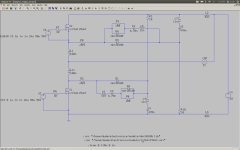
ZombieSS's power stage for Lebowski's controller video pg17

zombiess

10 MW
Joined
Jan 31, 2011
Messages
3,048
Location
Oklahoma City
Ok, this has been a very long time in the making. I had a HUGE amount of help from Highopes in learning how everything works and some of assistance with the math and a ton with the layout. I now have some idea of how involved these layouts can get and this one is just basic. I will forever be grateful for the education I have received on this forum because of others generosity. I hope I can repay some it back one day by contributing more.

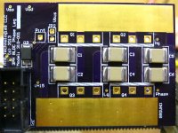
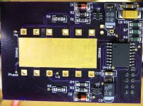
So in the zip file attached is my driver stage. It is based on a ST TD350E driver chip. I tried to incorporate reliability and fault detection into this, how well it works is yet to be seen. Highhopes has said he has had good experiences using this driver. This driver has been buffered to allow a gate drive of up to 14A peak current (2W power supplies instead of the 1W ones I am using would probably be needed to realize this level). The propagation delay of the entire setup should be ~500nS.

I have an open office document in the zip file that explains the basic circuit operation and what each component does, but I don't know if the part numbers exactly match up any more. I need to update it, so if you see something off, just ignore it or figure out what part number it's really referencing if you want to understand it. It was more for my own use than anything else to make sure I was understanding what I was doing.

In the zip file there is a PDF schematic of the driver section, low side and high side. Sub directories contain SVG images of the board layout sections, Gerber has the Gerber files and KiCad contains all the files that should be needed to open everything up in KiCad and look at it there.

Comments are welcome, but I don't think I will be changing much unless a major error is found somewhere. Sorry my layout is so sloppy, I just haven't gone back to clean it up as much as it needs. The net naming was done they way it is in KiCad to allow me to have the routing I wanted without it giving me errors.

I am hoping to be able to get a maximum of 200A peak from this layout. Once I have things working as a 6 FET I will keep adding FETs until I'm at 24 FETs. Once I max that out then I'll make changes from what I learned and go to TO-247 FETs, I left enough room to be able to build an 18 FET controller with the same board space. Reliability and failure mode detection were thought of during the design, it's one of the reasons each high/low section utilizes it's own isolated supply (6 for the driver stages, 1 for the brain board, 1 from the battery to supply 24V to the isolated supplies) and the only electrical connection between high and low side is the phase output. Everything is then optically coupled back to the brain board (which I'm currently redesigning to incorporate a PIC processor I am using to handle error processing). I am hoping this minimizes the chances of me nuking Lebowskis processors.

Anyway, have at it, you won't hurt my feelings. I'm just some guy with a High School diploma diving into a complex project.
View attachment TD350 Driver.zip
 
i'm anxious to see the results of your hard work :)
what is your build / test schedule?
do you have a collection of all the datasheets?

if anyone is interested, here are my cadence files (PSpice) to simulate the boost stage.
 

Attachments

  • GateDrive_TD350.zip
    31 KB · Views: 361
nieles said:
why do you have two 10k 3W resistor across your V_batt to gnd? could not find it in the notes
Yeh.. Im wondering this as well.

And do you know what part number you will use for the 1uf caps?
And are you only planning to run 6 1uf caps and 2 470 uf caps?
Or are you waiting to get a board built to test what you might need for caps?
 
Arlo1 said:
nieles said:
why do you have two 10k 3W resistor across your V_batt to gnd? could not find it in the notes
Yeh.. Im wondering this as well.

And do you know what part number you will use for the 1uf caps?
And are you only planning to run 6 1uf caps and 2 470 uf caps?
Or are you waiting to get a board built to test what you might need for caps?

10k 3w resistors are there to bleed the cap bank down after power off for safety, I will be working open frame for a while and not having to remember to discharge the cap bank every time is nice. There value will most likely change and one or none might be used. I have the spots created for their population if I decide to use one or both.

Yes, you are correct on the caps. Two 470uF and 6 1.0uF pulse rated polypropylene caps. I'll have to get back to you on the manufacturer and part number. I have some calcs showing that each stage only needed less than what I am using but I'll have to dig it up from my notes. Keep in mind this is one of 3 identical phases. These are low ESR electrolytic. If you add everything up you will see that the total controller will have around 2700uf of electrolytic caps across the rail and 24uf of low ESR ESL pulse rated snubber caps. I think I might have gone a bit overkill on the caps but I have a lot of them and they were cheap.
 
I guess it is an OK start when the first few questions about the design are about cap bleed resistors and not comments about bad layout and stray L. I guess I will see as more take a look.
 
now that's teamwork!

ps. zomb. don't worry, the weaknesses will reveal themselves when you put power & a real test :p
 
HighHopes said:
...don't worry, the weaknesses will reveal themselves when you put power & a real test :p

Without spending $250K with software and PhD teams to characterize stray inductance(s), the best way is to build and test. If there is a problem, IMHO that is where it will be. The solution would be a major redesign and not having the FETs all nicely lined up. The revision would have the high side FET(s), low side FET(s) and the 1.0uF cap all snuggled in nice and tight, getting "happy, happy, happy" with each other. (For example, 1 uF cap right from high side Drain to low side Source.) We find that "simple" mechanical layouts have higher stray inductances than "complex=expensive" mechanical layouts.

It is a system trade. You will know by test.
 
ZombieSS, great work!!

You know, I have spent a lot of time trying to figure out a layout better than just single in line (optimizing impedance, temperature sharing and ease of assembly), and concluded that as far as I can go, the best layout is still with MOSFETs in line on a heat spreader, but not all in the same line; the bottom ones inline and then paralleled with the top ones thus providing for near battery rails to put caps on.

By the way, does the 500ns latency includes the opto's reaction time?
 
Njay said:
ZombieSS, great work!!

You know, I have spent a lot of time trying to figure out a layout better than just single in line (optimizing impedance, temperature sharing and ease of assembly), and concluded that as far as I can go, the best layout is still with MOSFETs in line on a heat spreader, but not all in the same line; the bottom ones inline and then paralleled with the top ones thus providing for near battery rails to put caps on.

By the way, does the 500ns latency includes the opto's reaction time?

Perhaps in another revision. I decided on compromises for layout and packaging. Yes the Latency includes the optos which are high speed.
Thanks for the compliments.
 
Njay said:
You deserve them :)

I can honestly say that this is the single hardest thing I have ever tried to design. I would not have gotten it to this level without high hopes tutoring crash course style. I am just lucky that I have been granted the gift of learning most things at an accelerated rate. Ican never look at a switching layout the same way again. It really is as much art as it is science. I just hope it works when I build it.

I am thinking of building a dual rail layout at some point to see how it compares. All high side FETs on one rail, all low side FETs on the other. I actually have a board layout like this mostly designed, but the board was getting big because my driver was not as compact as this layout is. I will revisit it in the future once I get some hands on time. Nice thing about 3 separate phase boards is easy replacement if one goes nuclear leaving one or two still in a working state.

I will try to finish up the brain board and post it this week. I just received 70pcbs from OSHPark for throttle tamers so I'm going to be busy :lol:
 
Zomb, I thought I would share with you the base layout for a single phase leg that I am playing with. It's for TO-247 package FET's. They mount back to back on a half inch thick heat spreader that takes the heat up and out. If we all keep playing with this, eventually we will come up with the optimum layout so that the Chinese can copy it! :mrgreen:
12FetPhLeg-2.jpg
12FetPhLeg-1.jpg
 
Glad to see I'm on the right track :)
Although not naturally optimal concerning stray inductance, the in-line back-to-back does allow for close and easy mount of caps to overcome it. A heat spreader (instead of having isolation pad) will then care for more equal temperature. It's not a hard to mount topology. And then, finally, by entering power on one side and having the phase leave from the other we get to balance the current from a nominal point of view.
 
bigmoose said:
Zomb, I thought I would share with you the base layout for a single phase leg that I am playing with. It's for TO-247 package FET's. They mount back to back on a half inch thick heat spreader that takes the heat up and out. If we all keep playing with this, eventually we will come up with the optimum layout so that the Chinese can copy it! :mrgreen:
Yup Here is my next version.

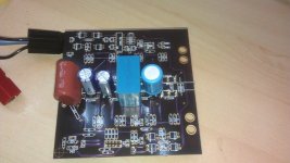
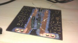
Zombies I'm not trying to screw up your thread. Just Showing the Simplest layout with best cap placement I can come up with. Very much like Dave's But
Mine will conduct from the body of the low side fet into graphite paper to angle copper or aluminum.
 

Attachments

  • 028 (800 x 450).jpg
    028 (800 x 450).jpg
    55.1 KB · Views: 12,447
  • 027 (800 x 450).jpg
    027 (800 x 450).jpg
    47.6 KB · Views: 12,446
Arlo1, bigmoose, thanks for sharing your board layouts. Gives me some more to look at. Arlo1... looks like you forgot your solder mask layer :lol: I almost did that myself, but I ran the layout through OSH park first while doing layout and figured out I missed it. I haven't sent the boards to manufacture just yet since I am still working on the brainboard for Lebowski's chip. I too thought about using the back to back layout on a single chunk of aluminum between them. I might try that out in another version, but not until I prove that this one is functional. That way I have the ability to compare differences in layouts.

bigmoose, what driver chip are you using? I am surprised to see you go with a combo high/low chip vs individual drivers and isolated supplies, but those might not be requirements for what you are doing. I only bring this up because I chose to incorporate them into my design after some discussions with HighHopes. He gave me the option on which way to go and the benefits of each and left the choice up to me. I decided to take the difficult, more expensive, takes longer to learn and understand method he was offering to tutor me in because I figure if I can get this all to work and document it, then I can always scale my design up/down to meet different operational requirements because I'll have a fairly solid base understanding to work from. That and I don't know if I will ever meet someone willing to give me this kind of education for free ever again in my life and shave years off my learning through educated guess/trial/error. I am glad that I did because because this has been an astounding learning experience for me even if my design fails for some reason. I feel my understanding of general electronics and circuit theory has doubled compared to just 2 months ago when I started on this and even then I had a good base working knowledge. I lacked the ability to explain the function of many components in a circuit, but now I can often figure it out, it's like a light bulb went off. I always sucked at repairing designs that were not my own, but now I have successfully been able to diagnose make repairs I wasn't able to do just a few months ago. Mainly on Xie Chang controller boards (I saved two 18 FET setups from the scrap pile that I purchased as scrap for $10 each because I wanted them for spare parts) so still FET driver stuff, but now I can look at a layout and finally understand most of how most of it is functioning and what a component is responsible for.

I am so excited to get going on this, but I found out my current day job as an IT contractor is ending either August 31st or Sept 30th... not sure which yet so I have to start looking for another gig which means less time to do this awesome work and probably relocating again.
 
zombiess said:
Arlo1, bigmoose, thanks for sharing your board layouts. Gives me some more to look at. Arlo1... looks like you forgot your solder mask layer :lol: I almost did that myself, but I ran the layout through OSH park first while doing layout and figured out I missed it. I haven't sent the boards to manufacture just yet since I am still working on the brainboard for Lebowski's chip. I too thought about using the back to back layout on a single chunk of aluminum between them. I might try that out in another version, but not until I prove that this one is functional. That way I have the ability to compare differences in layouts.
No I didn't I cleaned it off so I can buld up the traces. Do you think flowing ~300 amps though 1oz copper is good ? I will use some copper wire to build up the + and -
What I need is to figure out how to omit traces from having solder mask.....
 
Arlo1 said:
zombiess said:
Arlo1, bigmoose, thanks for sharing your board layouts. Gives me some more to look at. Arlo1... looks like you forgot your solder mask layer :lol: I almost did that myself, but I ran the layout through OSH park first while doing layout and figured out I missed it. I haven't sent the boards to manufacture just yet since I am still working on the brainboard for Lebowski's chip. I too thought about using the back to back layout on a single chunk of aluminum between them. I might try that out in another version, but not until I prove that this one is functional. That way I have the ability to compare differences in layouts.
No I didn't I cleaned it off so I can buld up the traces. Do you think flowing ~300 amps though 1oz copper is good ? I will use some copper wire to build up the + and -
What I need is to figure out how to omit traces from having solder mask.....

The solder mask layer allows you to prevent solder mask from covering that area. Download my KiCad files and you can see how I did it (because as you said 1oz copper isn't anywhere near good enough for 300A... or even 30A). Just upload the Gerber files to OSHPark and you can see how my high current areas are bare copper for building up the traces.
 
If we all keep playing with this, eventually we will come up with the optimum layout so that the Chinese can copy it!
they will copy only if it is cheap..

this was my first multiple discrete mosfet design (i always used modules when more than 1 mosfet per switch was required). i thought about it a lot how to do the layout. i know you want to keep the mosfets per switch all on one heatsink so they share same temperature rise & cooling and can self stabilize through temperature coefficient. otherwise, all options were considered. i thought about in line, per phase, square, sandwitched. in the end, i think it matters not too much because in all variations i found the limiting factor was simply that their size forced the geometry to have poor parasitic inductance & balance. this fact will eventually lead to a power limitation. paralleling more discrete mosfets is not practical because of severely limited diminishing returns (safety margin when paralleling is not linear). so to get higher power, i.e. for electric car, out of a conventional gate driver & discrete mosfet will be a challenge most difficult to solve. i have some unconventional ideas that i'm kicking around but its not worth to discuss at this point. let's see where we are with zomb. 4 mosfet per switch topology first :)
 
HighHopes said:
If we all keep playing with this, eventually we will come up with the optimum layout so that the Chinese can copy it!
they will copy only if it is cheap..

this was my first multiple discrete mosfet design (i always used modules when more than 1 mosfet per switch was required). i thought about it a lot how to do the layout. i know you want to keep the mosfets per switch all on one heatsink so they share same temperature rise & cooling and can self stabilize through positive temperature coefficient. otherwise, all options were considered. i thought about in line, per phase, square, sandwitched. in the end, i think it matters not too much because in all variations i found the limiting factor was simply that their size forced the geometry to have poor parasitic inductance & balance. this fact will eventually lead to a power limitation. paralleling more discrete mosfets is not practical because of severely limited diminishing returns (safety margin when paralleling is not linear). so to get higher power, i.e. for electric car, out of a conventional gate driver & discrete mosfet will be a challenge most difficult to solve. i have some unconventional ideas that i'm kicking around but its not worth to discuss at this point. let's see where we are with zomb. 4 mosfet per switch topology first :)
I think about this all the time... And finding 3000 amp mosfet modals seams hard... :) So One Idea Im toying with is having a motor split to 6 or 9 phases... Actually 2 or 3 seprate sets of windings that do not connect to each other. Then the Inductance per set can be higher (good thing) and the Amps per phase set can be lower by 2 times for 6 phase and 3 times for 9 phase. So you will have 1 main inverter with all the sensing and 1 or 2 dummy inverters which will just pulse as a copy of the first one. This will allow say 6 mosfet bricks of say 800 amps run each set of phase wires so 800x3 is close to my goal of 3000 amps... Of course its not cheep but I am looking for muscle car power and it will take some creative thinking with what's available with todays component
 
I had a look at some of the files, what strikes me is that the design all concentrates on the driver side of the output stage,
while all the problems we've seen in Arlins thread come from the high voltage / high current side. I use IRS2186 drivers
with about 10Ohm gate resistor per FET, and don't see any reason to change as there's no problems with this. All the problems
stem from stray inductances combined with high currents in the output side of the power drivers.
I know the layout looks small and compact etc but, electrically speaking, it isn't. I've measured quite large voltages across
just the legs of FETs, let alone the extra distance the current has to travel because of FET spacing.
So.... use a fuse ZombieSS and remember, the bigger the fuse the louder the bang (above 20A, wear earplugs !)

I've been working on the output side of the power stage, but due to me being in a mechanical phase of the hobby at the
moment haven't had time to try it yet (been mating my AF motor with my recumbent).

What I want to use is fast switching the FETs but in combination with the 'philosophy' that during turn-on the FET should
see an inductance and during turn-off a capacitance. This makes you can switch as fast as the driver allows, 100ns or less
dependent on driver strength. This is the schematic I want to try when I get the time:
messing_around.jpg
the 11nH and 42nH inductors are capacitor internal and power wiring (just 10cm parallel traces in a 6 FET!). The 180nH's are intentional
added inductors. I1 models the motor.
Lets say the current flows into the controller,the top FET just switched off (but carries the current in its diode). When the bottom one
switched on it sees the 360nH, it can switch on very fast and while there's still no current flowing through it (no switching losses !).
Now lets look for when the bottom FET switches off. The current through the inductors wants to keep flowing, with the FET off
it flows through C3 D2 into C1. Due to the caps the voltage on the drain rises relatively slowly meaning the FET can switch off
while it has 0v across it, again no switching losses. The voltage across C3 will rise quickly to the supply, at which point D1
starts conducting. Now C1 will pose a heavy load for the current, meaning that the voltage across C1 will only rise 20V or so above
the supply.
Interesting is that during all this the current still flows through L3, meaning there's no big transient across the supply like you would normally
get. The effects of the 11nH in the caps, it will give a spike but measurements will need to be done to see how severe this is...
 
your thoughts are well understood. the gate driver and power pass sections are married to each other and you're only as strong as the weakest link. a good gate driver but bad power pass = failure. a bad gate driver + good power pass = failure. it is sometimes hard to tell where the real root of a problem is because of the overlap. what appears to be a problem with power pass could be solved in gate driver and vise/versa. in the end, you have to pay attention to both & give it your best go.

having said that, i am all in favour of further experimenting & discovering other solutions that are better. your discussion sounds a lot like resonant inverter (zero votlage, zero current switching) topology. I have built two of these before and basically what i found was that it was great solution for 1kW or less but the margin of errors get so tight at higher power it was too difficult to control and so i resorted back to conventional solution (and suffering conventional problems). i hope you have much better luck and please be sure to post when you do! :)
 
HighHopes said:
i'm anxious to see the results of your hard work :)
what is your build / test schedule?
do you have a collection of all the datasheets?

if anyone is interested, here are my cadence files (PSpice) to simulate the boost stage.
Whats R-23 for?
 
Arlo1 said:
if anyone is interested, here are my cadence files (PSpice) to simulate the boost stage.
Whats R-23 for?[/quote]

R7, R10, R23, R26 are all 0 ohm SMD resistors that might be used for altering gate resistors. Easier to add an additional resistor in series which trying to find the correct gate drive resistor size and allows for multiple combos with just a few resistors. Basically they are there to save time during testing/tuning. They are also non inductive type.
 
Back
Top