Ebike Battery Monitoring and Control System

Progress with DipTrace

The pc board layout is pretty near complete, but I need to "do it right" and enter a schematic. So I started that yesterday.

I've just about finished the schematic already. It went pretty fast, though there are still incomplete items like some of the pad layouts. The library has a lot of parts, but often not the ones I need. DipTrace has very good tools for making parts so it doesn't take long to make or adapt one for what is needed. I haven't read the documentation, but occasionally a Google search is useful to answer a question.

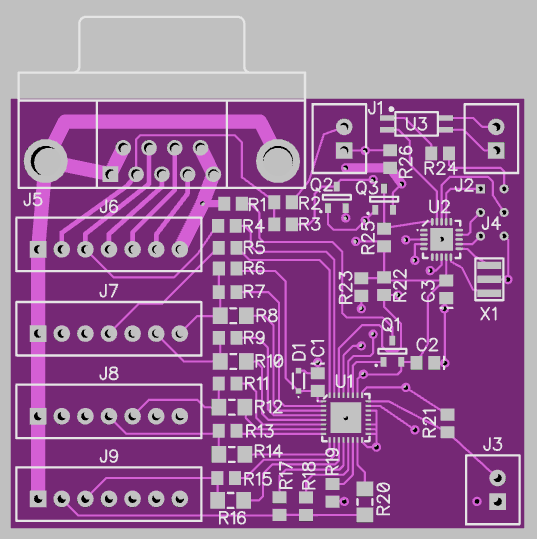
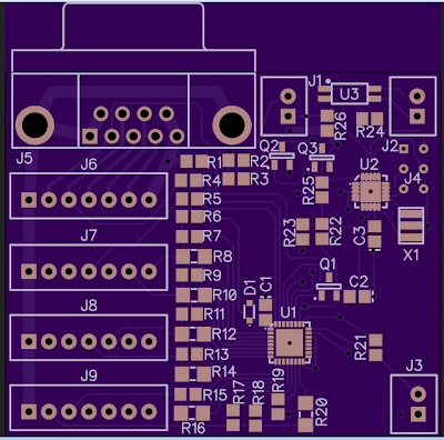
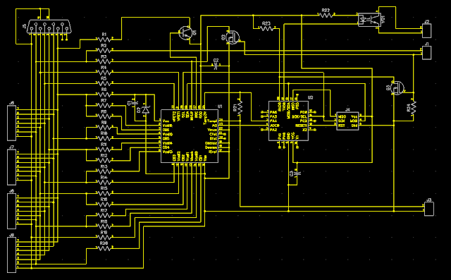
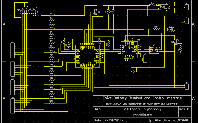
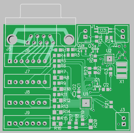
Here are some screencaps that show what it looks like. Schematic, and then the PCB layout.

batt%2520ifc%2520r028a%2520sch.png


Batt%2520Ifc%2520r028a.png


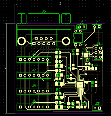
I see the ceramic resonator is still missing, I haven't found or made one of those yet. The layout has very few vias, it has been reorganized for that. The ground plane is not poured in this capture. The layout is autorouted, so the traces have not been widened up for current handling except for two there that are still locked from earlier experimenting. I'll tune the routing later, right now I re-autoroute frequently so don't want to customize things yet.

Here's the essence of this design at this point:

Intersil ISL94208 6S front end chip with analog mux/offset/scaling, balance driving FETs (not using the charge/discharge control part of the chip)
AVR Micro, 16K with TWI/I2C and real USART for easy serial and standard ISP pads for programming
Daisy chained optically isolated serial connections, in and out, resonator to make serial stable without calibration
Resistors for balancing, but the current will have to be kept low enough to avoid heat issues, "Gentle Balancing", probably 50 mA or so
AVR is powered off when the board goes into sleep, current per cell should be less than a few 10's of microamps at room temperature
Intersil chip is woken up by incoming serial, AVR chip is then powered by the Intersil chip's 3.3V regulation system
The master will wakeup and query these slave battery interface boards, requesting data and sending them balancing instructions
The plan is for these slave boards to time out and shut down if they are not being communicated with
One slave board will be required for each parallel 6S group, so 12S would require 2 boards, 18S - 3, 24S - 4
Connectors for 4 parallel 6S packs on each slave board (JST-XH)
More than 4 parallel packs is possible by using cabling or external paralleling boards for the balance lines.
The master can be most anything like a common Arduino or Teensy or Raspbery Pi, lots of possibilities there
DB9 is a diagnostic port for tapping into the cells for external measurements and balancing (don't plug in your pc serial here :shock: )
Connector for thermistor for pack temperature monitoring is provided, thermal shutdown possible in software
Board is about 2x2 inches, small enough to integrate closely with the pack

Any questions, comments or suggestions appreciated.
 
I let the software do a parts placement and board layout automatically, and it consumed more than 50 square inches of pc board space! Quite entertaining and un-optimized.

Here's the schematic, coming along nicely. It is cleaned up, and now what remains is to detail the parts with things like the proper pad layout. Most are done but a few remain to adjust. Then we can do a new layout and organize it back down to about 4 square inches.

DipTrace is lots of fun to learn and use.

batt%2520ifc%25206s4p%25202013r0.png
 
Progress Update

Adjusted the parts placement and, after a few iterations, got it back to 4 square inches (a bit less than 2 inches by a bit more than 2 inches). It was useful to have done the layout incrementally before, not sure I would have done as well working directly from the full schematic. There are a few more parts on the board than before, so it is a challenge staying in this size, but it is reasonable.

Spent time adjusting things to get the routing fairly tidy, adding the groundplane pour back in, etc. There will be some final iterations, but it is reasonable now. There are more vias than I'd like, about 20-25.

Have gone through most of the parts and made/adjusted the pad layouts to be precise. Just a couple more to go.

There is room for 5 parallel balance jacks if the jacks are close spaced, I'm planning to go with 4P and keep the wider spacing. It makes it easier to unplug things when the spacing is open.
 
DipTrace has a 3D rendering engine built in. I don't have any parts models so just the board is rendered. It has a VRML output, but the image above is just a portion of a screen capture from the built in rendering viewer. Just push the 3D button in the layout editor and that pops up. Nice to see what the board is going to look like.
 
I spent some time going through the layout and "cleaning up" the traces, fattening up the parallel tracks for the cell balancing, and doubling up tracks to the DB9. I also changed the pinout of the DB9 to use two pins for ground and two pins for +25, as well as heavier traces so we can put in more current via the DB9 for "external charging and balancing" if we want to.

I need to review the ceramic resonator. It is a bit large, and I need to determine exactly which frequency and precision to use to make precise baud rates and trouble free operation with no "tuning". We will have to calibrate the Analog channels, that is unavoidable, but there is no reason to need to adjust the frequency if we specify it right.

That may be enough to be ready to send in the Rev 0 boards. :)
 
Resonator (and CPU) Frequency

One source of serial clock error is the CPU clock frequency being divided down for the USART. 4.00 Mhz is what I've been planning to use, but this is not quite the correct frequency. But how far off is it?

The margin for clock error is about 2-3 percent for an 8 bit serial transfer, regardless of baud rate.

One thing to note is the Arduino also uses an 8 or 16 mhz clock, and it suffers in most cases from the same error as using a 4mhz clock causes. At 2400, 4800, 9600 and 19200 baud this error is 0.16 percent. This is small enough to fit in the error budget when talking to a "correct" clock such as likely found in a PC. Talking to an Arduino or Teensy 2.0 will not suffer this mismatch since both CPUs are using multiples of 4 mhz.

So I can safely select a 4 mhz ceramic resonator.

Now to find a good small one with a footprint that allows some choices.
 
I tried to post this last night but something went down - could not get Picasaweb to finish the download.

Here's OSH Park's rendering of the board, complete with gold plating:

batt%2520ifc%25206s4p%25202013r0%2520oshpark.png


I wonder if this view is really the top soldermask rather than copper, the fine pitch pins on U2 seem to be bloomed. I can't get back to all the different views of the board now, unfortunately. I also see that C1 is a bit close to U1. I guess we'll find out in 2 weeks!

It came in under four square inches. So these three boards were cheaper than getting my Moped tire changed. :)
 
Good to know about Laen.

This is a Rev0 prototype board, I'm sure I'll find a number of things to improve on my side. Already see a couple, but that's normal for a PC board design - as soon as submitted something pops up.

I'm so glad to now have a toolset and manufacturing process that allows me to get arbitrary size small boards designed and made at low cost! For a long time I've used ExpressPCB's low cost 2.5 x 3.8 boards which was limiting, and often I panelized smaller designs onto it. There are a number of small boards I want to do and this will be excellent. I see some things I'd like improved in DipTrace, but I have not learned all the features, and it provides a lot of capabilities that ExpressPCB did not. Perhaps I'll try Eagle again later when I have more time...

The 3D rendering of the board looks OK so I expect the board will be too, at least I don't expect manufacturing flaws will be a big problem.

The big problem is finding all the time to complete the test and development cycle, designing the board is the fun/easy part. :wink:
 
Nice reflow oven project. That's the direction I was thinking I might go, but the one thing I had not looked into yet was the Infrared toaster ovens. That makes it more costly but should be better for this purpose. I see that the heat may not be even though, unfortunately.

I have an IR preheater, one thing I was wondering is if I get two of those and mount them facing each other, they have lots of quartz tubes so the heat is even. The area is pretty small though, and they are not all that cheap, so it would probably not be the best approach.
 
I've used a cheap ($30) toaster oven from Target quite successfully. It has little shields around the heating elements and I put the boards on an aluminum cookie sheet to even out the temp, works quite well. For actual production I would use an actual controller, but for prototyping it works fine with just watching the temp carefully.
 
I used one like this:
41sX0NzPqTL._SL190_SY246_CR0,0,190,246_.jpg


The front opening infrared toaster ovens are nearly impossible to get in the UK. I bought mine wholesale and it was cheap, about $30 in US dollars.
 
So now that hardware is coming, I need to complete the BOM and get parts ordered, and think more about the comm protocol and software.

This is a work in progress, so this posting may be edited or superceded later.


Communications Protocol (proposed)

Terminology - During this discussion there are two kinds of communicating objects - the "Master" and the battery interface "Nodes". There is only one Master, there can be several Nodes, each one serving a 6S block of parallel batteries in the present design. So a 12S system would have two, an 18S system would have three, and so on. The Master originates all activity - waking up the Nodes and initiating their Reading and Balancing.

The communications link is an optically isolated serial daisy chain, so the Master sends something to the first battery interface Node, it receives that and sends something to the second Node, and the final Node sends back to the Master. This arrangement minimizes the hardware and addressing issues as Nodes don't need to have addresses. The order of Nodes is by convention to be starting from ground and working up, though for most purposes it does not matter. But if you want to know which voltage corresponds to which cell it will be easiest if they are in the conventional arrangement.

The essential functionality needed, roughly in descending importance is listed below. This assumes that calibration is handled by a separate program ahead of time and that normal Node software will not have that feature, but will just use the pre-determined calibration. Calibration will be addressed in a separate posting later.

Essential Functional Requirements for Communications

Wakeup battery interface Nodes (from their normal low power sleep state)
Request cell voltage and temperature readings
Request balancing activity

Wakeup requires a serial "space" signal for a minimum of 60 milliseconds to trigger the Intersil battery front end chip to awaken, which turns on the 3.3V regulation and powers up the Micro, plus the time to boot it up, or about 80 milliseconds total. So each Node should send out an 80 millisecond space on its serial output as it boots up to get the next node in the chain up and running. At the end of this period it should send out an "I'm awake" message. This is for the Master to see the chain of interface boards is fully awake and ready to run. The Nodes should copy the "Awake" message on their input through to their output so the Master will see them all. Nodes reset a timer on serial communications and go back to low power sleep after 5 seconds without communications, so the Master must constantly poll them at least once per two seconds (up to 5 times per second). A Wakeup cycle will then take about 80 milliseconds per battery interface Node. This will be done at bike turn-on and at the start of a charging cycle, and the Nodes kept awake during the charge and discharge cycles.

Reading cell voltages is the most important job of the battery interface Nodes. This is a noisy environment, so many readings will be averaged to get the best we can from the hardware we have to work with. I haven't decided exactly how that is going to be done, so I'll make a choice and potentially change it later after the repercussions are understood. Taking readings is going to take time, possibly turning balancing off temporarily (this is a control option, can be done either way), configuring the multiplexer, waiting for settling, taking a number of readings, re-enabling balancing, and averaging the result, and doing this six times per Node to get all cells. Balancing will alter the reading results, so turn it off during the reading process. We want to read the cells at close to the same time so we need to trigger the reading process on all Nodes. The "Reading Trigger Message" is short and is forwarded by each Node, so it flows through quickly and back to the master, so it knows all nodes have started their measurement process, and the master sends the initial "Readings Ready" message to the first Node where it sits until that Node's readings are ready. Let's assume for a moment that the reading and processing cycle takes a bit under 100 milliseconds. After taking and preparing the readings each Node will forward the Readings Ready message on through. Then about 100 milliseconds after the master sends the Trigger it receives the "Readings Ready" message from the last Node which indicates that all Nodes are ready and then sends a "Reading Request Message" to request the data. Upon seeing the "Reading Request", each Node sends its reading data message (containing all of that node's readings) and after that forwards the reading request message. Each Node forwards any Data messages on through. So the master gets back a set of Data messages followed by the Request message. They come back in the order the Nodes are connected, first Node first. The Master reviews the data and takes care of any low voltage or high voltage issues so the Nodes don't worry about thresholds or cutoffs. The temperature readings are included with the cell voltages data.

For cell voltage readings the messages contain a 16 bit field per parallel cell group. Scaling is arbitrarily chosen such that all ones corresponds to 5.000 volts, and all zeroes corresponds to zero volts. The calibration process will map actual readings onto this scale. Averages of multiple readings will be accumulated in an extended precision sum and scaled to this 16 bit result by the calibration factor. Atmel document "doc8003" discusses "Enhancing ADC resolution by oversampling" that has helpful information on using additional conversions to extend resolution. Later on testing will reveal how helpful it is in terms of resolution enhancement, but in any case taking averages of readings will help with noise reduction and any occasional bad readings. The above document indicates that four readings per bit of resolution extension is required, so if we want to get 12 bits of resolution it would require 16 readings, and 16 bits of resolution would require 4096 readings! In this case we have 8 values to read (6 cell voltages and 2 temperatures), and a 100 mS window, so 10 mS per value. The maximum ADC clock rate for good resolution is 200khz and a conversion takes 14 clock cycles which in this case is 70 microseconds. In 10mS this could make 140 conversions. So making 128 conversions would be possible and would produce approximately 13.5 bits of resolution (if all the other conditions for this are met, which is unlikely). But this is a reasonable starting point for the averaging. Note that this will produce a 17 bit sum, which can be handled with 32 bit arithmetic. Using a 64 sample sum will produce a 16 bit total and thus might be a better choice, or at least an easier one. Also Mux settling time is required. It may become desirable to push the temperature readouts into a separate message at a lower readout rate and focus the highest rate on the cell voltages if needed.

Balance control messages are sent about once per second by the master when balancing is engaged. Each Node has six balance resistors, so a byte is sufficient for each Node with a bit for each cell/resistor. Balance messages have a byte for each Node, and as the Node is processing the message it will remove its balance control byte, so the message gets shorter as it passes through the Nodes. The empty balance control message is sent but not passed on; if a Node receives one an error message is sent instead, so it should reach the Master empty if it had the right number of Node bytes to start with. Balancing requests time-out in about 3 seconds, so the Master must renew them every second or so.


Message Summary

Wakeup pulse (80 millisecond space), master sends to start wakeup, each Node forwards as it boots
Awake message, Node sends after Wakeup, ignore on input
Reading Trigger Message (with balance on/off selection)
Reading Request Message
Reading Ready Message
Reading Data Message
Balance Control Message, contains a byte for each Node with 6 bits for the balance on/off requests
Error Message

Format of Messages

Message Starting Marker byte
Message Type code byte
Message Data Length byte
Message CRC check (two bytes) (six byte min message)
Message Data bytes (0..32 bytes) (determines buffer size)

Message Data Sizes

Minimum message 6 bytes
Maximum message 22 bytes (so far)
Reading Data: 6*2 + 2*2 bytes (six voltages, plus two temperatures, all 16 bit data)
Balance Control: <nodes> * 1 bytes

Baud Rate Impacts

Use slowest baud rate that gets the job done (for noise immunity)
9600 baud is about 1mS per byte (for reference)
Short message 6 mS
Data message 22mS; 24S would have four Nodes, so total time would be about 100mS
Cycle time for 5 hz would be 200mS, so 100mS for trigger and measure, and 100mS for transfer would be about right

Serial Configuration

9600 baud, 8 data bits, 1 stop, no parity
Discard byte on framing error
Timeout after a few char periods and discard message if remainder missing?
Discard messages with bad CRC
Receive FIFO buffer 64 bytes plus two indexes (interrupt based receiver fills FIFO)
Receive message processing buffer 32 bytes plus length byte
Transmit processing buffer 32 bytes plus length byte (wait to clear before refilling, interrupt based transmitter?)
Processor RAM 1024 bytes (AtTiny1634) (of which 132 bytes will be taken by these serial buffers)

Recommended Cycles

During Charging or Discharging keep Nodes awake by polling after waking them up
During off periods allow Nodes to sleep in low power

Wakeup Cycle:
Master asserts "space" condition on the serial out line for 80 milliseconds
Nodes boot up and pass the "space" condition on through the serial daisy chain net
Master waits for incoming space condition (one framing error followed by one "Awake" message for each Node in the chain)

Master Loop:
Master sends balance control message (optional, required to refresh any balancing activity)
Master sends Reading Trigger message, waits to receive it back
Master sends Reading Ready message
Master waits for Reading Ready message while readings are taken, about 100 mS later this arrives, (Master should read current during this period)
Master sends Read Data Request
Master reads all the node data and the Request (25 mS per Node)
Cycle repeats

Other Possible Features
Read Cal Factors
Read Raw
...

eof
 
Back
Top