Futterama's power stage for Lebowski's controller IC

yep, all correct. But, the 0x8000 is actually 0x0000 with the MSB inverted. Taking his into account 0x7FFF works out as 0xFFFF, or -1. And 0x8000 becomes 0x0000, so 0.

Your calculation for erpms is also correct.
 
I have been playing with the controller. I have added 14awg wire from FETs to current sensors and 8awg from current sensors to the motor (I had those 8awg wires lying around with the right connectors attached).

I thought the motor ran a bit rough, it was noisy and shaky, so I re-calibrated the current sensors. When calibrating several times in a row, the results can vary greatly. Anyway, the motor was still noisy, so I ran the FOC measurement with the same settings as I have done before, and now the chip says around 25µH instead of 4µH. So I redid the FOC calibration and during calibration, the motor got quite loud and the negative lead on my DC link capacitor went glowing red hot.

So, something must be wrong. I have been loading the motor a bit with my lathe chuck. It has a hard time getting the chuck moving but I did manage to get it going. I only ran it for something like 30 seconds total. During that time, the controller seemed to lose the motor at one point, there was a fraction of a second during an acceleration where the motor kinda lost power but regained it quickly. This was after I changed to the bigger wires.

Lebowski, when working with this, it would be really nice if the setup menu had an option of turning one FET on at a time so it would be easy to find a FET or gate driver that doesn't work. If one FET is shorted, and the check for standstill is disabled along with pins 5, 7, 8 grounded (basically "shorted FET detection" is disabled) then it is hard to find the defective FET without a test function because the PWM test would give shoot through. I imagine a menu where each FET could be turned on/off manually. And if the circuit on pins 5, 7, 8 was there, the chip could find the defective FET automatically and report this to the user using a menu option for that along with the manual FET test options.
 

Attachments

  • new_wiring.jpg
    new_wiring.jpg
    43.5 KB · Views: 3,175
  • hot_cap_lead.jpg
    hot_cap_lead.jpg
    35.5 KB · Views: 3,175
Did you find the blown FET ? Can't you just measure the FETs with an Ohm-meter with the controller off and not connected to a battery ?

About the current sensor calibration, when you're not using HF you don't need to calibrate, just reset to default and leave it at that.
 
Ok, I could scope my way to it, the blown FET affected the signal going to it's gate, so I could see it when scoping the gate drive outputs and also when scoping the phase wires. It's a highside FET, and from what I have seen scoping the gate driver outputs just now, I'll have to do some more scoping after replacing the FET to make sure the bootstrapping is working as it should even under load. I won't spend much time improving the bootstrap gate drivers, I need to move on to isolated gate drivers where I have some fancy plans for the isolated power supplies or rather supply.

I suppose the FET couldn't handle the abuse from pulling the lathe chuck, the whole setup did get quite hot. The current limit was still 100A and I should have set it to 50A which is what I expect of it to be able to handle. I think it would be a good thing to have a small PIC with a display that could poll RS232 data from the chip so I could have a look at the phase current and erpms realtime during testing.
 
Detecting the a fault can be handled by using a better gate driver. A better gate driver could most likely prevent the fault from happening in the first place. When learning it's a good idea to use a gate driver with some protection features as it can save you the hassle of popped FETs, at least it has in my case, probably 20-30 of them. This number is not counting the ones I purposely tried to destroy while testing shoot through protection, I never succeeded so I never damaged one. To this day I have not blown a single MOSFET on anything I've designed, but I have had numerous faults detected.

Desaturation detection can possibly save the MOSFET from an over current/overheating issue because the RDSon of the MOSFET increases with temperature. That high resistance causes the desat detection to trigger at a lower current level. It's not a replacement for good thermal practice and monitoring/fault handling, but it's sort of a bonus that it works in tandem to trigger at a lower current as the MOSFET heats up.

The gate drivers are easy to check, just disconnect the MOSFET and run the controller in PWM test mode, scope each output. If you get PWM the gate driver should be OK.

The issue you have with the rail capacitor is caused by too much ripple current. You can calculate the amount of capacitance and the ripple current that is required for your load conditions using this information HighHopes compiled and posted in another thread.

View attachment DC Link Capacitor Selection.pdf

I'm trying to create my lab notes which are mostly scattered in PM conversations and posts on this site. I've downloaded most of the info and am trying to compile it all into a detailed easy to read format that I would like to someday put together into a how to / best practice guide. I've got lots of great formulas for calculating the right component specs for most gate driver parts and power stage parts. Gate drivers design requires detailed specs.
 
A small update. I came across a circuit for the isolated gate driver power supply that has the potential of being small, simple and cheap. I'm working with HighHopes to figure out the details, and when it is finished, I'll post it here for everyone to copy and use.
I have already tested the basics on breadboard and it's looking promising :D

Details will follow when we are satisfied with the design and component choice.
 
Another small update. I have been away from this project for too long so I went back to look at the gate driver supply I'm building.

I'm getting help from a local Field Application Engineer from Linear Technology to use their new 
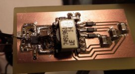
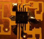
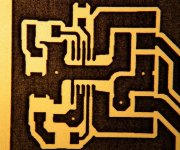
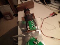
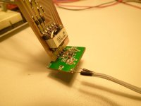
LT3999 - Low Noise, 1A, 1MHz Push-Pull DC/DC Driver with Duty Cycle Control to drive a 1:1:1:1:1:1 push-pull transformer from Würth Electronics. He sent me some samples in DFN package, so I just learned new PCB fabricating and soldering skills, the pads are only 0.25mm wide and spaced 0.25mm and I nailed it in the first attempt, both when etching the PCB and hand soldering the 3x3mm part 8)

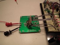
The PCB has the LT3999 chip, a few capacitors and resistors to support the LT3999, and the Würth transformer. There are also diodes and capacitors at the output from the transformer.

So basically what I have here is an isolated DC/DC supply with 4 outputs. The idea is to let 3 outputs drive the 3 highside MOSFET drivers, and the last output should drive the 3 lowside MOSFET drivers. The diodes are arranged so that the 3x highside supplies get power from one half of the push-pull switching cycle, and the single lowside supply get power from the other half of the push-pull switching cycle. This way, the power is distributed evenly over the push-pull switching cycles. And since the 3 lowside MOSFET gate drivers share their GND connection through the lowside MOSFET source pins, I can get full gate driver isolation using only 4 isolated supplies e.g. 3x1W for highside and 1x3W for lowside.

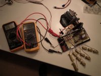
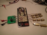
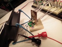
Regarding the wattage, I have just done some load tests on the outputs and I see 4.2W on the single lowside output and around 1.3W on the 3 highside outputs, a total of around 8.2W. I should be able to push this to a total of 10W as the datasheet have some typical application circuits with a 10W output so the LT3999 should be capable enough. Maybe I need to use a slightly bigger transformer as the one I use now gets quite warm, so does the LT3999 but that is due to my poor thermal management on the homemade PCB, this will improve with a professional fabricated PCB with power planes and vias.

I will be making a new PCB, preferably after I receive some MSOP package devices that should be easier for me to solder. I will use a bigger Würth transformer on the next board too, to see if that can make a difference on temperature, efficiency and output voltage/current.
I will also receive a demo board from Linear so I have something to compare my own work with.

The Linear Technology push-pull drivers also has the potential of being the driver for an isolated DC/DC supply for my Lebowski chip - with an inductor on the output, the voltage ripple can get as low as 100µV - for a 5V supply, that's 0.002% ripple! :shock: :D

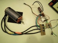
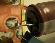
Ok, enough talk, let's see the pictures!
 

Attachments

  • setup.jpg
    setup.jpg
    59 KB · Views: 2,894
  • pcb.jpg
    pcb.jpg
    53.8 KB · Views: 2,894
  • dfn_soldered.jpg
    dfn_soldered.jpg
    73.7 KB · Views: 2,894
  • pcb_layout.jpg
    pcb_layout.jpg
    112.1 KB · Views: 2,894
More update. I received the demo board today. I did some tests and measurements on it as it was delivered (dual isolated supply +12V and -12V, both 200mA output with ripple elimination from inductor and LDO regulator). It got pretty hot, PCB reached 51°C with the lowest input voltage so the LT3999 is supposed to be hot, good to know :D
So, I made 3 new transformer boards that would replace the demo board transformer and output stage so I could use the LT3999 on the demo board with my own transformer and output stage, simply because currently the demo board offers the LT3999 better thermal management than my own board.

As of now, I have only tested with the next bigger transformer from Würth (I have 4 sizes, only did test on the smallest until now). It does seem pretty good. I removed the duty cycle control from the demo board to allow for full duty cycle, and I need to remove the overvoltage lockout (OVLO) to get higher input voltages than the demoboard default of around 15V (the LT3999 supports up to 36V input) but with 15.3V input at 630mA, I get around 12V out, thats a total of ~9.6W in and ~6.6W out, only 3W power loss in the LT3999, transformer and rectifiers which is ~70% effeciency, pretty good I think 8)

Next step is testing with the rest of the transformers, remove OVLO and test with higher input voltage and higher wattage output. The LT3999 is designed for up to 15W output according to the product video I saw yesterday :D
 

Attachments

  • demoboard.jpg
    demoboard.jpg
    64.7 KB · Views: 2,874
  • demoboard_setup.jpg
    demoboard_setup.jpg
    55.6 KB · Views: 2,874
Great, I just killed the demo board, did nothing than raising the input voltage slowly to find the limit and suddenly at 21V, nothing, no output from the LT3999 switches :(

The LT3999 has current limit on its switches and built-in thermal shutdown, so I don't get why it died. I had a fan blowing on the board to keep it cool.

The good news is I reached a measurement of almost 9W output at 13.3W input with the second smallest transformer.
 
HAHA! I managed to replace the LT3999 by cutting up the demoboard only leaving the necessary components and board space, and heating the whole PCB on a bigass soldering iron, using it as a hot plate :mrgreen:

It works again! This time I need to attach a heatsink since the board has shrinked from 75x75mm to 20x25mm which affects the thermal performance of the board.
 

Attachments

  • heating_pcb.jpg
    heating_pcb.jpg
    36.7 KB · Views: 2,820
  • small_demo.jpg
    small_demo.jpg
    49.4 KB · Views: 2,820
As a tip: you can use a simple low cost household clothes iron as a hot plate for soldering and de-soldering. Solder melts below 200 C while irons go above this temperature. Back when i worked for philips research clothes irons were used for baking chips, they told us it was the cheapest and best hot plate around...
 
Really great tip Lebowski, thanks!

The bigass soldering iron I have, is not temperature controlled, so it just keeps getting hotter, actually too hot today, the PCB got a bit of brownish glow to it, so it was HOT. A household clothes iron is temperature controlled, but probably not with actual temperature values, but I have a probe for my Fluke multimeter I can use to write actual values to the iron.
 
I added a heatsink to the backside of the PCB using some noname thermal pads and two screws. I used the same 12V 80mm fan as before. This is much much better, the heatsink really does a great job. The heatsink is cool to the touch and the LT3999 is not getting so hot I can't hold my finger on it.
I'm now running 13.3W input (19V, 700mA) and a total of 11.5W output, which equals 86,5% effeciency! The extra cooling must be good for the LT3999 switches :D
 

Attachments

  • pcb_with_heatsink.jpg
    pcb_with_heatsink.jpg
    65.8 KB · Views: 2,806
Nice job!
 
I got myself a $13 clothes iron today. On the highest setting, I could barely melt fresh solder on the iron itself and it would not liquify solder on a small PCB. My Fluke temperature probe showed around 150°C. So I took it apart and did a small modification to the thermostat so now the lowest setting is around 215°C which seems fine for a small PCB. I did not mind taking it apart, I don't need the handle and water tank for steam anyway. So now I'll build a wooden case for it, so it lies level and I need the case to be big enough for it to support my hands on the side for accurate placement of the IC.

The tip of using a clothes iron as hot plate, is the best tip I've got for a while now. Many thanks to Lebowski for this awesome tip! :D

Pictures will follow when I have built the case.
 
You tube reflow. Toaster oven and there is also people using the electric frying pans. I didnl mine with a toaster oven and manually adjusted the temps while watching the time. It worked perfect.
 
Lebowski said:
What wouls be neat to try with the hot plate is to get a flux pen and some solder paste and try to solder a complete pcb in one go...
That's what I did with the toaster oven and I saw people use the electric frying pan for it too. These things are <$10 at a thrift store like valuevillage.
Its so fast. Took board assembly time from ~6hr down to ~1.5 hours.
 
Back
Top