HighHopes
10 kW
- Joined
- Mar 28, 2013
- Messages
- 929
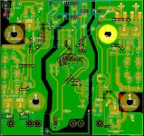
The via u put for desat, are you maintaining creepage? I can move the ground plane back I was relying on the clearance settings to keep it safe but Its better to change that.
i already helped you on what creepage is, how to know what you need, what reference to use, how to identify any problems in your design and how to solve. you have already all the tools you need to figure it out. i only raised the question cause it looked odd, i did not measure or look in detail.
actually, that's how reviews are normally done.. the reviewers rarely look in detail, they just are given one day to review and of that day only have time about 1 hour.. so they just use their experience to look for things that are "odd" or "not normal" etc. and raise question "did you look into that" or "do you have this problem?" or "why did you chose this cause i never seen that before?".