DIY 6FET Controller help

Assemble my circuit and did a little test and looking look so far.
There is no fet connect yet so the voltage on the desat cap will climb until it
triggers desat, but at a new threshold voltage that will hopefully be way more stable.

I was only using a 5.1v zener as a Vref for this test as I still have to order a Vref chip.


Lebowski said:
Futterama said:
SjwNz said:
and see how much current it takes before it blows it up.
Remember safety goggles and gloves 8) :shock:
and earplugs :D the bigger the fuse the louder the bang, 30A is already a firecracker !


Yep, I learnt about exploding MOSFETs and IGBTs many years ago
Safely glasses and ear plugs are my friends.
 
I spend most of the weekend doing Desat tests , I made a basic 1/2 bridge setup and
fitted my gate driver to the Hiside FET and then connected the G/D of the Lowside fet together to
keep it off. I then used a old PCB from one of my customers, and converted into a Pulse generator.
Using a trim-pot I could adjust the output pulse width from 3uS to 60uS which was triggered by
pressing the button. I also had a input to look at the Desat fault output from the 333J which
would turn on some LEDs when a desat fault occurred.

View attachment 2

After doing some tests I overloaded the 200Amp current sensor, so added a 0.005ohm resistor
for a current shunt and measured Desat currents around 250amps into a 10uH inductor.
The pulse width was 30uS and the desat kicked into action around 25uS.

After confirming the circuit was working, I disabled the extra comparator circuit I added
and just used the desat feature of the 333J.

I then replaced the coil with a short-circuit and with a supply voltage of
50V I was getting currents upto 800- 900Amps ???. Shutdown times where around 7uS so I changed the
Desat cap to 33pF and got the Desat shutdown time down to 5uS.
I was very,very surprised with the currents I was seeing. I done this test up to 30times and
the FET is still working.
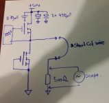
ShortCct test Cct.jpg

I then looked at the switching speed with the scope connected to the Source of the hiside
and it was around 200nS. From reading posts on ES this maybe a little bit to fast?
so added a GS cap of 10nF and it made no differents (did not try any higher values).
(gate resistor, 30ohms On, and 10ohms off)
I will play with this more when I build the controller if I need to slow down the switching due to spikes or ringing.
View attachment 1


I was using 2 x 470uF caps for these tests, so removed one of them which dropped the Desat current by approx 100amps So I saw an issue with having too much DC link caps. I still need to learn how to calculate the DC cap capacitance but I think even one 470uF cap is to much.

So I did one more crazy test. I added the 0.005ohm resistor between Lowside fet and GND
and turned on the lowside fet using a battery. I pressed the pulse button
to turn on the Hiside fet and saw a peak current of 1200amps. Are these currents real?
Whats going to happen if I made a controller running up to 100V in the future. The desat currents would be crazy hi.

View attachment 3

I also did the same test above without the 0.005ohm resistor and connected the scope across the DS of the Lowside fet
and used it as a 2mOhm resistor but got some silly value of like 2000amps so decided this reading was a bit dodgy. :?

Voltage across 5mOhm resistor from Crazy test above.
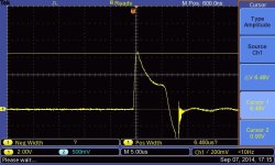
Crazy test current 6.4V  across 5mOhm.jpg


One more test I did was to heatup the driver board while connected to the 10uH coil.
at room temperature desat triggered at 244amps, and with the driver board to 60°C
desat current only dropped by 20amps.

So after this weekend I have decided to not worry about the extra circuit I made to make the Desat threshold more stable ,
I can now make my gate driver board smaller, and maybe I am getting to worried about the desat current in a shoot through event.
I have all ready showed the fet can handle lots of shoot through at those mad currents a number of times and its still going.
I am picking there are lots of controllers out there with not desat and the ones I have heard of , peters running for 1.5years , Lebowski's 10,000kms
are still going , so the number of times desat could occur are so small , my controller could last many years.
Its still nice to know I cannot ? :) blow it up.

I will start building the power stage and then it may take some time to get use to using the dsPIC, as the last time I used one was 6years ago.

Time to watch DoctorWho now.
 
Playing with desat, seeing the crazy currents involved and realizing it's stopping you from blowing up your MOSFET is an enlightening experience is it not?

You may never need it, but if you do, those few extra components really paid for themselves :)
 
SjwNz said:
So I did one more crazy test. I added the 0.005ohm resistor between Lowside fet and GND
and turned on the lowside fet using a battery. I pressed the pulse button
to turn on the Hiside fet and saw a peak current of 1200amps. Are these currents real?

There are definitely very high currents, but part of it is probably a fake glitch on the oscilloscope due to its relatively low CMRR (common mode rejection ratio) at high frequency.
At high voltage and high dV/dt the potential of each node on the board change temporarily due to the quick rearrangement of the charges, even the board GND is not stable compared to the oscilloscope GND. This moves the common mode voltage on the oscilloscope probe, and a glitch is seens on the screen added to the real differential signal.
To find the extent of this issue, just short the probe's GND and signal together and connect them on a node on the board (can be GND or any other), and do the test, if there is glitch, then it is due to the low CMRR. It can be eliminated or reduced with a high speed differential active probe or differential measurement with 2 channels of the oscilloscope.
 
Futterama the fets I am using are IRFP4468PBF .

Playing with desat, seeing the crazy currents involved and realizing it's stopping you from blowing up your MOSFET is an enlightening experience is it not?
You may never need it, but if you do, those few extra components really paid for themselves :)

After using MOSFET for years doing crappy little jobs like just turning on a small loads or making little PWM speed controllers , I have a whole new outlook
at what they can really do now. So this has been very enlightening .

So I did another test tonight, first I wanted to see what the true? RDSon was for the LowSide fet. I still had the 5mΩ resistor in series with the Lowside fet
so did a Shoot through test and recorded the voltage across the 5mΩ resistor. I then did the same test but measured the voltage across the lowside fet.
From this I worked out the RDSon for the fet was 3.3mΩ. I then removed the 5mΩ resistor and connected the Lowside fets Source directly to the -BUS.
With two DC link caps of 470uF I did a Shoot through test again and recoded a voltage across the lowside fet of 5.3V ÷ 3.3mΩ = 1606amps.
After taking into account the CCRM (thanks for that peters) I ended up with a peak current of 1490amps and the Fet is still working.

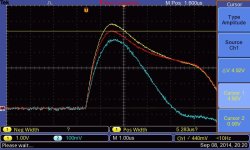
After doing your test peters there was a 300mV difference, so I connected CH1 across the FET and CH2 for the CMRR. Pressed the Math button and setup CH1 - CH2
and this is what I saw. I think this is the first time I have ever used the Math button on a scope :oops:

CH1 Yellow = Voltage across Fet with RDSon 3.3mΩ ?
CH2 Blue = Probe connected to its gnd lead and then connect to the Source of the Lowside fet.
Red = CH1 - CH2

CH1-CH2 1490Amps deset test.jpg

How is this fet surviving this when it has a Pulse current rating of 1100amps.

I am getting some 5uF PP caps tomorrow so will try them out instead of the Electrolytics.
 
While playing around with layout ideas , I was thinking of having 3 gate drivers in a row with another 3 gate drivers mounted above . so the lower 3 maybe for the Low-side fets and the upper 3 drivers for the Hi-side. But I was thinking about how to make connections for desat to the mosfet board.
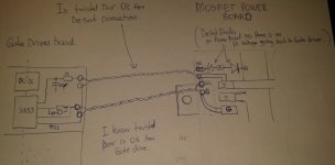
The picture below is how I plan to make the connections, does anyone see any issues with this?
I know its ok to use this for the Gate drive , but not sure about desat connections.
I decided it would be better to leave the Desat diodes on the mosfet board so there would be no HV going over the desat twisted pair wires.

Remote Desat Connections.jpg
 
HighHopes told me to keep the desat lead under 4" (100mm) for twisted pair connections. I'm not 100% sure on the reasoning of 100mm length though. My guess is the length relating to inductive coupling / noise possibly causing false triggering, but that's just a guess on my part.

For driver to silicon I was told a max of 6", 150mm.

Pretty sure these lengths would vary depending on power level, amps/volts in use on the switching side.
 
its fine to use twisted pairs, but why? seems this design would be better off on ONE pcb?
yes one of the wires is redundant, in theory, but in practise it is nice to twist signal wire with its reference when available. for what its worth, i have run a single wire from desat, not twisted, to adjacent gate driver 4" long, switched 600V in 100ns; worked fine.
 
For a low inductance you need to have the return wire next to the signal wire... so I would say that if both signals are departing the board at different locations and running separate, the lowest inductance is with a return wire twisted on each signal wire (both return wires connected on both ends).
 
HighHopes said:
. for what its worth, i have run a single wire from desat, not twisted, to adjacent gate driver 4" long, switched 600V in 100ns; worked fine.

Well, now I know where that 4" length recommendation comes from :)
 
its fine to use twisted pairs, but why? seems this design would be better off on ONE pcb?
Mr HH, I found a Diecast box at work thats a bit smaller than the case I was using and worked out
I could fit my controller into it, but have to break the PCB into 2 sections.
Not sure if its a good idea but will give it a try as I like this new case.
 
Desat signal does not actually need to be low inductance because it is not high pulse current.

This second statement is hard for me to justify but my intuition says that it is better to bring the signal as a single wire without a ground reference no twisting. The desat signal is very noisy if you twist a ground wire with it you risk coupling the noise. But then again I rely a lot on the high-quality gate Drive ic to be very robust interface. I guess I am saying I would rather have high noise at the single gate Drive desat pin then lower noise all over the gate Drive ground which is everywhere. I have also done this many many many times.
 
So, if you use a separate board to fit in your special case then you will have one pair of twisted wires going to gate source of the MOSFET. And a single wire coming from the source pin to the gate Drive PCB diode cathode. The diode cathode will not have a ground reference underneath it there will be no copper under that part. And also keep in mind that is high-voltage at the cathode so be mindful of your creepage. You should have at least 1 cm space between the twisted-pair and a single desat wire.
 
HighHopes, I found and started reading a thread of yours on Ivan's Garage.
I am only on Page 2 but saw a section about DC-Link caps which has been very handy.

Stiff bus during fault detection:
If your gate drive or phase current sensor has some sort of fault current shut-down, then the cap must supply the fault current for as long as it takes for system to detect fault and tell MOSFET to open. 10uS? The bus voltage is not allowed to drop more than 20% during this time or else fault shut down may not work properly.

I was about to make this mistake above by trying one 5uF polypropylene Cap. I did a test with the 5uF and Desat worked but
the bus voltage dropped a crap load.
 
HighHopes, I found and started reading a thread of yours on Ivan's Garage
ya that's what happens when you google search "Miracle Genius"

i'm continuing that EV design with zombiess but in the background. he's ready to learn system integration and willing to do the actual hard work that i can not do (bench test & test drive) so that's good. there are a lot of things to think about when you start to design a system. when we're done we'll post it all online, well, at least the "basic" full up EV motor drive. i hope also that we will collect all the messages back and forth (i save all my emails) and we can abbreviate our discussions into a more streamlined "how to design, build and test a high performance motor drive". we've been at this for over a year now.. so don't hold your breath :oops:
 
Been a bit busy so not much progress.
After a couple of people suggested using one current sensor to measure the phase current instead of the 3 sensors on each phase output, I was a bit unsure about this as I did not want to add anything between the Fets and Busbars just in case it would cause some issues. After thinking about this over the last 3 days I came up with the following which I think will work fine. The Current sensor is between the DC-Link caps and fets and i have
kept the busbars laminated (I think). The only other thing I am a bit worried about this the total capacitance of the snubber caps which could be 1uF to 3uF.
The snubber caps are next to the Fets and maybe this will hide the peak phase currents from the current sensor or is there not enough capacitance to worry about.
The other reason I have been thinking about using a single current sensor for this this controller is that it will only be a Sensored design.

Hope my attached drawing makes sense and any thoughts on this would be good.

View attachment SingleCurrent Sensor for Phase Current.pdf
 
your layout looks really good... except for the current sensor. it is not good to add impedance, however small, between DC link cap & mosfets. its a really bad idea.

$0.02
 
SjwNz said:
The only other thing I am a bit worried about this the total capacitance of the snubber caps which could be 1uF to 3uF.
The snubber caps are next to the Fets and maybe this will hide the peak phase currents from the current sensor or is there not enough capacitance to worry about.

It's not a problem. Depends on the phase current, but imagine you cut the power bus before the snubbers (remove the battery and the DC link caps), then from I*dt = C*dU, at I=10A and C=1uF the bus voltage would drop by 10 Volts within 1us, or by 100V at 100A. If the battery and DC caps are there, then after only a small voltage drop on the PCB trace inductance, the current starts via the sensor. So the snubbers cannot supply the bridge for a long time, its filtering effect is low. But they are required to supply the MOSFET internal capacitors: during the edge transitions the charge is taken from them more than from the DC link caps through the PCB trace inductance, and they smooth the inductance current.
 
You can put the sensor between the battery and that the dc link capacitor but not between the capacitor and the MOSFETs.
It is extremely unlikely you will ever convince me otherwise :)

Having said that I recognize your power level is low so maybe you can get away with bad architecture, it's just not my style to do that
 
HighHopes said:
You can put the sensor between the battery and that the dc link capacitor but not between the capacitor and the MOSFETs.
It is extremely unlikely you will ever convince me otherwise :)

Having said that I recognize your power level is low so maybe you can get away with bad architecture, it's just not my style to do that

I'm not trying to convince you, but what is the role of the dc link capacitor? For me there are 2:
- to provide a low impedance power supply close to the bridge
- to filter the PWM, so on the battery cable the current is more or less flat (at least not a square but a filtered square current)

But the ESR of these caps are ~0.1 Ohm (btw it is similar to the battery internal resistance), and have some serial inductance, too. This is not very low, so they are not really effective against the PCB trace impedance on the board, this is why the snubber caps are needed.
The serial resistance of this current sensor is 0.1 mOhm, it is 1000 times less than the ESR, so to me the DC caps can be reasonably anywhere between the power connector and the bridge if the board is this small sized, it has only minor effect. The power plane lamination coverage is also not 100% at the sensor, but it can be improved if the sensor is placed more over the power plane.
Don't you agree?
Due to the little effect it is true that for very high current and power, when there are more MOSFETs and larger board, for sure it is better to distribute the caps close to the bridge, then the current sensor placement must be also different.

SjwNz, anywhere you put the caps, I think the 2x220uF is probably too small, they can heat up due to the ripple current and also may blow up, even if they are low ESR, a few 1000uF would be better.
 
Hi Peter appreciate your response. As you said the capacitor has the two rolls and then about five more after that (less important). As for capacitor resistance, think of it more of it as an impedance. What is the impedance at the frequency you want this capacitor to play it's many rolls. What frequencies well at see for each role for that matter? At what frequency, impedance, will that capacitor fail to be useful enough to accomplish that role?

Long story short, do not put the capacitor there
 
Back
Top