EZ PCBs: DipTrace PCB Design Software

Alan B

100 GW
Joined
Sep 11, 2010
Messages
7,809
Location
San Francisco Bay Area, USA
This thread is for people interested easy ways to design PC (printed circuit) boards, specifically using DipTrace software and submitting boards for low cost online PCB manufacture to places like www.oshpark.com.

It is NOT a thread for bashing or arguing about which is the "best" Electronics CAD software, though comparisons of specific features might be useful to those trying to understand what DipTrace is good for, as well as it's limitations. So let's not get caught up in what is "best" (which is undoubtedly some high end package we cannot afford at home), but instead in what's useful for our purposes. If you want to argue about what is the "best" then open a new thread in the toxic area and have at it. :)

So, if you are using (or have used) DipTrace, please join in here and let us know how it is working for you (or not and why), and maybe answer questions from others who are considering it, or trying to learn it.

If you are interested in DipTrace, it is certainly best to search the web first but if you don't find an answer perhaps you can join in the discussion here and ask your questions.

There is a DipTrace support forum, that is perhaps a better place for really deep technical questions. Or perhaps that expertise will develop here.

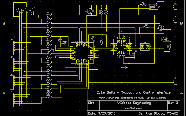
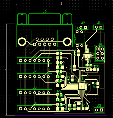
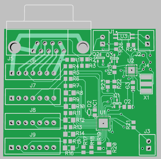
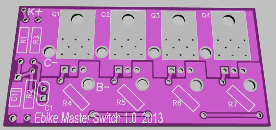
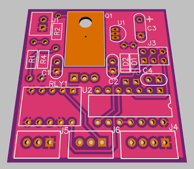
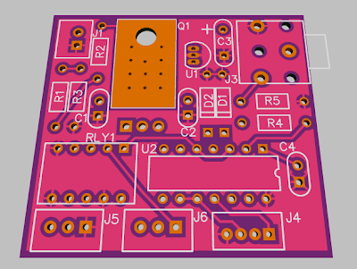
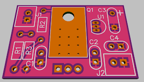
For those who don't know what DipTrace is, it is an Electronics CAD package that includes schematic capture and PC board layout. It is commercial but has free versions with fairly useful limits, and a graded price schedule so you can buy more capability if you need it, and easily add to it later without cost penalty. So the price varies from zero on up depending on your needs. This type of detail changes with time so it should be obtained from their website, http://www.diptrace.com. It is a fairly low price package, as an example presently prices start at $70 for a license that allows 300 pins, two signal layers, no board size limit, has autorouting, etc, and this allows commercial use (the same limits as the free version but allows commercial use). So you can start for free, and then if you decide to sell your invention you can license the package, but if your not selling your stuff you can continue using the free license, it does not time out. For me this is good to learn the tool at no cost and do some projects, without a major cost barrier if I decide to go further.

Most of my ECad tool experience has been with ExpressPCB, which is free and easy to learn but only allows you to send boards to their board house, which is convenient but not always cost effective. So I was looking for something more flexible that would allow me to send boards anywhere (such as OSH Park which has a good deal on low cost boards). I tried FreePCB for a few boards, which works okay but is really basic, having no schematic capture or autorouting, and I wanted more. I very briefly tried KiCad (which is open source which I really like), but it was difficult to learn and I had some problems with it. I looked at Eagle which is probably the most popular low end commercial package, and decided the learning curve was steeper than I wanted to tackle at this time. I heard about DipTrace and reports that it was fairly capable and yet quick to learn, and I chose to try a few projects in it. I'll probably learn Eagle later on, but for here and now I'm focussing on DipTrace.

I'll say more about my current experience with DipTrace later on down the thread.

So who is using or considering DipTrace? How's it going? What is it doing for you?
 
Here is my current DipTrace project. I started learning DipTrace part-time a week ago, and inputting this design-in-progress:

batt%2520ifc%25206s4p%25202013r0.png


This is the layout as of a couple days ago:

Batt%2520Ifc%2520r028a.png


I'm pretty happy with the progress. This is part-time though I did spend quite a few hours on the weekend with it. To be fair I did a small simple board over a year ago in DipTrace, but I didn't remember much of it when I started this layout a week ago. On the earlier small board (much simpler than this board) I only learned part of the DipTrace software package. So it looks and feels like fairly reasonable progress. This time I've used much more of the program suite, making component and pattern libraries, schematics and circuit board layouts.

I'm using the built-in autorouter which is fun, but in the end I'm going to have to do a bit of trace fixing. Still the autorouter is doing most of the layout work. The auto-parts placement was a poor joke. The board I designed is four square inches, with the auto placement it occupied 60 square inches!

I sent a small test board to OSH Park a few days ago to check out DipTrace and OSH Park working together. I didn't rename the output files (which they suggest), as an experiment I just zipped up the Gerber layer and Excellon drill files as they came from DipTrace and uploaded them to OSH Park's website tool. They were recognized and rendered, so I sent it to production. It takes about 2 weeks to send a board back, so I've another week or so to wait. The OSH Park prototype processing is $5 per inch and you get three boards. So it is really $1.67 per square inch of board and you must get multiples of 3. They panelize them and make 3 panels. The amazing thing is that first class shipping is included in that cost, and no sales tax. They also have a small run production capability at $1 per square inch in multiples of 10 with a minimum of 150 square inches in combined designs. For details see their website http://www.oshpark.com. They also have a library of PC boards that you can have made, about 500 different designs (at the standard price $5 per square inch for 3 boards).

I've done some boards with a similar service at SparkFun called BatchPCB. They have a nice system and low pricing also for panelized boards. Their turnaround was a little slower and their pricing a bit higher, making OSH Park very interesting.

I'll report more on that when the test boards come back.
 
DipTrace has a 3D rendering tool built in. I don't have models for my parts, so it just renders the board. It is useful to get a good look at how the board will look:

batt%2520ifc%25206s4p%25202013r0%2520b.png


I've been working through "finishing" the layout. Now I've stopped autorouting, or at least stopped ripping up all the routing and starting over. Now I'm customizing traces, so I don't want to lose that. Here is some of what I do to finalize a layout:

Verify component selections
Verify hole sizes and component pad layouts
Check current handling requirements
Fatten traces to increase current handling where needed
Double up traces (on both sides) to increase current handling as needed
Increase clearance
Adjust groudplane as needed for best effect
Make sure things are solderable, avoid soldering to the groundplane as it is a big heatsink and difficult to solder to
Add strategic vias to get to the groundplane
Adjust component locations to improve the groundplane
Adjust component silkscreen to make it more readable and understandable
Verify clearances and wiring (built in tools to do most of this)
Look for silly routing, improve it

Adjust some traces to intentionally act as fuses in specific cases - for example avoid an external connector going straight to the groundplane, insure a trace is separating it so if there is a fault the current will be much lower.

The good news is that DipTrace allows setting and adjusting things nicely, the bad news is that these settings get lost when you "unroute" a trace, and I haven't seen an easy way to get the software to remember this. You can avoid doing "unroute all" and just unroute the traces you are working on, leaving the rest routed as-is.
 
Another handy tool in the PC layout process is a Gerber viewer. Gerber is the most common file format for the PC board design, and once you design a board it is prudent to review it carefully both in the layout program, but again in a separate program that views the files being sent to the PC board house.

gerbv is a free Gerber file viewer. I have not tried others, many of them are not free. This one seems to be fairly popular and do the job.

www.gerbv.sourceforge.net
 
So here I am a little over a month out in part-time use of DipTrace. I've been spending more time on it than I expected for a variety of reasons, but it is still limited to some evenings and weekends. I've designed quite a few boards at this point, and some of them have come back from fabrication. Testing is just getting started but the boards look fine.

So how do I feel about DipTrace now?

The learning curve was quick for me. I had fiddled with it a little before, but not significantly, and I had forgotten most of what I had learned. Most of my previous experience was with ExpressPCB which is pretty trivial, and DipTrace works differently so it didn't really prepare me all that much.

There are four programs in the package, one each for pc board schematic, pc board layout, component schematic and component pcb layout. They are all graphical, but you can get to coordinates when you need to be that precise.

There are libraries of parts that are helpful, but they often don't have what you want. So the ability to make and adjust your own parts library is important, and DipTrace does this amazingly well. Laying down rows of pads in different arrays is truly quick and easy.

Thermal vias are not well supported, they promise this in the next version. They seem to make one major release per year.

The schematic editor is adequate though a bit quirky. Deleting a connection isn't completely controlled, it deletes the whole original wire, I don't see a way to cut off just the end or to unstick it and reconnect it which was easy in ExpressPCB. But it gets the job done and is fairly easy to reorganize in terms of moving things around to make it look reasonable.

The component layout had one annoying property. Changing the hole spacing shrank the component outline to wrap the holes and lost the previous dimensions. This should be fixed, a lot of work goes into making the outline just the right size, and even when locked this is lost when changing hole spacing.

The dimensions are great for getting things the right size, you can add them where you care and lock them to the corners of things so as you adjust them they read out the actual sizes.

On to the main course, the PC board layout program. I like this one. It is so amazing to put in a schematic, finding and making parts as you go, and then click "convert to layout". The parts locations were a joke, but to be honest I spent no time tuning the parts layout feature, I just grabbed the parts and relocated them myself, watching the ratlines to help guide the process. Rotating parts and watching the ratlines helps to choose orientation for best PCB compatiblity. Then hit autoroute and watch it go. I'd call parts placement "poor" and autorouting "fair" and quite useful. moving parts around, unrouting all or part of the board and then re-autorouting is quick and easy. Eventually you hand adjust traces, and hand route some while re-autorouting others, and you get to a reasonable board that is electrically correct in a surprisingly short time.

Along the way you can touch the 3D button and get a quick rendering of the board (and parts if you have 3D for them). It is a great way to "see" the board, and built in!

Copper pours are easy to do and work well. There are some issues such as pours of different priority won't join even though they are on the same net, hopefully they will fix that. But you can make complex shaped pours that will handle most situations. It would be nice to have a button that "updated all pours".

Lettering doesn't get as small as I'd like, but it works well.

Exporting files to Gerber/Excellon was easy, and I was very pleased to discover that OSH Park accepts these files directly, I didn't have to rename them to Eagle standard names. It would be nice if they had a way to save all the files into the required zipfile directly, but writing them and moving them into a zipfile is not all that difficult.

Rules checking, schematic verification, and connectivity checking are good and quick. Be nice to have one button that triggered them all.

Updating a part's pcb layout is a bit tedious, you need to modify the layout in the layout program, save it, re-attach it to the component in the component diagram program, save that, update the part in the schematic capture program, save that, then go to the pc layout program and refresh from the design to have the new layout in the PCB. It is easier to do than writing it, but a lot more than you'd expect, and figuring this out the first time can be frustrating.

With this package it is quite possible do design a small board and send it out for manufacturing in an hour or several. Just perfect for those little projects that you would rather have a PC board for instead of a rat's nest of skywires on a perfboard. Especially when you need two or more of them, or wish to share with others. :)

Someday I'll tackle Eagle, but for most things DipTrace is quick to learn and gets the job done, and the free version goes a long way, and the prices to upgrade are low, plus they are differential, you can always apply what you have paid for toward the upgraded version. If you are an Eagle user you may have no use for DipTrace, but if you have been wanting a better PCB program but have been putting off the big Eagle learning curve then DipTrace may be just what you need to get going quickly and be productive without learning dozens of command line options. DipTrace is all graphical and what you see is what you get!
 
Hi Alan, Actually I am using the KICAD for the PCB designing and now I want to try the Dip Trace and I want to know in the beginning should I go with the free trial or should I buy the license and what are the features for free version?
 
Start with the free trial, not many limits on it at all.

That way you don't have to spend money until you are more certain to need to.

I haven't hit any limits in the free version, don't recall what they are at the moment. Layers and pin limits as I recall, but not that small or tight. Features are all there, autorouting, 3D modeling, etc.
 
Back
Top