i2c BMS for hobbyking lipos

smev

1 mW
Joined
Jan 4, 2014
Messages
19
Ok so in search of a easier way to manage lipo batteries, I have decided to design my own bms system. I would like to get a production run done of some nice smd boards.

So pretty much looking for how many people would be interested in purchasing.

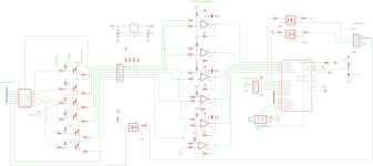
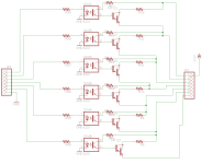
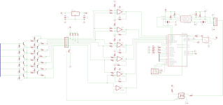
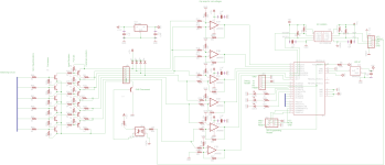
What each board would do is have a read out of the individual cell voltage to 10bit. 6 cells per board. The output on each board will be a isolated i2c interface allowing up to 128 boards on the same 2 i2c wires. The i2c address and firmware will be programmed via a spi adapter.

There will be a expansion port to connect a cell balancer for people who want to shunt the cells while bulk charging. This will be controlled by the isolated i2c inteface as well.

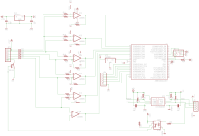
The boards will be controlled by a atmega (arduino compatible), that will combine the cell readouts from all the boards and enable shunting, cut charging, alarm on low voltage etc.

A optically isolated mosfet will control the power of the circuit. So the circuit will be fully powered off when not in use.

The point of the i2c interface is to go digital and verify that all cells are reading proper, if any cells are wildly out of range, we know that something is wrong and to abort the charge, or alarm on low volt.

So just tossing around some ideas, I will post some schematics if people are interested.
 
I would be interested.
Any idea of the price per 6cell board?
 
Here is a rough schematic of the cell monitor board.

I still need to calculate a few resistor values, but for the op amp resistors they will be all the same value, around 100k ohm. Also not all parts have been selected yet. So the ICs might change a bit. I am using the atmega644 for prototyping but planning to use the smd atmega328 on the production run.

Pin out of the board is VCC, Enable, SDA, SCL, GND

I figure we can keep the cost lower then $20 per board.

As for the shunting system. It is just a optocoupler -> tip122 mosfet + resistor on each cell. I want to keep this separate to keep the cell monitor small, and also so people can adjust shunting and add heatsinks etc.

Speaking of which.... how many people are bulk charging and need shunting anyway ? Personally I just disconnect series and charge on a high end charger.

Also if anyone wants to help out with routing the pcb, or help deal with the manufacturing part that would be awesome.
 

Attachments

  • schematic.png
    schematic.png
    25.8 KB · Views: 1,575
Couple of suggestions for you after glancing at the schematic:

1. Good idea using a precise voltage reference, you will be happy you did.

2. I would suggest choosing some more efficient components. The LM358 will use around 1mA supply, 7805 will use a few mA and has a minimum recommended load to maintain regulation. If you're going SMD then there's no reason not to go with more efficient parts. A few mA here and there add up quick, and you don't want to drain your cells if you forget to unplug the BMS. Not a problem for development, but if you want to actually use it long term then efficient components are a must. Every 1mA of quiescent current will drain 1Ah from your pack every 7 weeks or so. My quick count from looking at your design is that you have at least 5-10mA of quiescent current that could be largely eliminated.

3. Loose the input diodes, the drop across each one will be imprecise and vary depending on temp, load current, etc.
 
And here is the shunting board schematic. The cell monitor would mount to this board bed of nails style. The shunts are controlled by the output pins of the isolated microcontroller.
 

Attachments

  • shunting.png
    shunting.png
    9.5 KB · Views: 1,725
Yeah I was wondering about the input diodes. I'll remove them from the inputs. Maybe I'll put some diodes on the power to allow for lower cell count packs.

As far as components, part selection hasn't properly been done. Components were just mostly selected because they were in the eagle libraries and have same pinouts to the parts I will use.

Need a different power regular anyway as probably over voltage on the 7805.

For power usage, there is a mosfet on the gnd connection to cut all power when the circuit is not in use. So just power up, take readings quick, and power off. This way it should have no drain on the pack when the system is off.
 
I used the LM285-1.2 on my single cell monitors, only a 1% device but still plenty accurate at normal operating temp. Combined with oversampling the ADC to 12-bit I was able to consistently measure within a couple mV of what my fluke DMM showed. To minimize power draw I used one of the micro output pins to drive it so it could be turned off when not in use. I was able to get total power consumption down to under 10uA taking 4 readings per second.

Have fun, I'll be following with interest.
 
Yeah I don't think its going to be that efficient on the power usage. The atmega will probably pull 10ma on its own. And if driving the shunting mosfets its going to need some extra power. So just going to the route of cutting the gnd when not in use so power usage shouldn't matter too much.

I have to power the op-amps from full battery voltage since I'm comparing each cell.

So at single unit pricing:
ATMEGA328P - $4.45
3x LM358 - $0.51 - $1.53 - opamps
ISO1541DR - $5.40 - i2c isolator
MAX6107 -$1.28 - volt ref 0.4%
MMBT2222A-TP - $0.16 - npn for shutdown
TCMT1107 - $0.88 - optocoupler for shutdown
MC78L05ACHX - $0.59 - 5v power regulator 100ma
20x - 100k 0.5% resistors - $0.07 - $1.40

Already up to $15.69 + a few cheap parts, of course prices go way down in bulk.
 
Are you physically cutting ground? Unless you have some mechanical switch that's toggled on/off, you are going to be drawing current, 10mA will draw a battery pack down in no time. You can easily get the ATmega current down to almost nothing by sleeping it. I would also be concerned about forgetting to turn off the switch and killing a pack or forgetting to turn it on and killing a pack, or worse starting a fire. Even if you're the only one to use the thing, you have to assume every type of usage scenario will happen. Sorry if I'm critiquing your design too early in the process, but these are all things I've had to deal with myself.
 
i'm always interested in bms solutions. especially if they provide some output to an arduino (or are even managed by it). this makes it possible to monitor the cell's value from the outside on a smartphone (via bt) or a dedicated display.
what is the maximum current for charging and discharging? or is this meantto monitor only?
 
The gnd is cut by the MMBT2222A-TP NPN transistor should be a almost non-existant leakage (T7). The schematic has the npn where it grounds back to the battery. I can put a timeout on the microcontroller to make sure the bms is always shut down.

How this setup would work is one atmega would be reading the voltages over i2c and switching the charging current on and off. If the cells are too high, the charger would just turn off and wait until the cells are within range. Since its all digital we can start discharging the high cells earlier into the charge and hopefully use a lower rate.

I have been playing around with some parts and around a 200ma-500ma shunting current would be really cheap to implement. The hobbyking battery medics do a max of 450ma so should be able to get similar performance with no heat sinks. I figure the packs shouldn't be more then 10% out of balance unless they are abused so the balancing should be minimal.

Here is a updated schematic, diodes have been added to for power to allow packs from 3s-6s. As well as a simple balancing circuit.
 
smev said:
The gnd is cut by the MMBT2222A-TP NPN transistor should be a almost non-existant leakage (T7). The schematic has the npn where it grounds back to the battery. I can put a timeout on the microcontroller to make sure the bms is always shut down.
My point about cutting ground was that if you disconnect the ground from the lowest cell potential, then what is ground referenced to? You can't have an indeterminate ground. There's no reason to disconnect the cells to save power if you use power efficient devices in the first place. It may not seem like it now, but it will be much simpler and more reliable in the long run.

Also, you'll want to add pull-down/pull-up resistors between the base-emitter pins on your NPN/PNP transistors to guarantee they turn off properly. Something around 10k is usually a good choice. More important on ones not connected to the ATmega pins since they have built in pull-ups that you can use.
 
Well the real gnd is the negative on the battery, the atmega and opamps are essentially the load for the mosfet. The schematic may be a little confusing with how I have the gnd net. When power is applied to the enable pin, the optocoupler switches the npn to start sinking current to the battery gnd. There is not really any suitable microcontrollers that use low enough power.

A alternative solution would be to use a isolated dc-dc power supply, and power the bms externally.

There is the ADM3260 that is isolated dc-dc and isolated i2c on one chip, availability isn't the best and its fairly expensive.

I added the pull ups and pull downs. The atmega only has pull ups and are controlling npn, so I added in the pull downs on the control pins as well. I think the only thing that is missing is a few capacitors on op amp power, and volt ref power.
 

Attachments

  • schematic3.png
    schematic3.png
    57.7 KB · Views: 1,537
smev said:
There is not really any suitable microcontrollers that use low enough power.
Sure there are. The ATmega328 (and others in the family) are extremely low power in sleep mode, I've measured actual average current draw down around 8uA for the same basic application you're using it for. 8uA is approximately 1Ah every 14 years, better than the self-discharge rate of the cells.

smev said:
A alternative solution would be to use a isolated dc-dc power supply, and power the bms externally.
That would eliminate the risk to your pack, but whatever auxiliary battery you use would have a relatively high drain since most isolated supplies have a minimum load required for isolation. A suitable LDO connected across all the cells will be very effective in this application and will eliminate the problem with uneven current draw.

Regarding isolation, I would advise that you add an unisolated header as well for debug.

[EDIT] Check out this page on sleep modes from Sparkfun. Not comprehensive, but a good starting point.
 
Well another problem is the op amp resistors that form the voltage dividers, they cannot be too high of a value or the op amps don't play nice. So there will always be some drain there. Unless the gnd is disconnected, theres going to be at least 0.5ma wasted just by the op amps. I think the enable pin solution is probably the best.

I added a resistor values and a few caps. Also a serial debug header. So time to start criticizing my resistor values lol

So on the schematic, the 12v net is the full voltage of the battery. the 5v is the regulated. The gnd net is switched by the T7 mosfet to the real gnd. The VCC and GNDA nets are on the isolated side.

Also added in resistors to cell 1 just to keep draw for all cells perfectly even.
 

Attachments

  • schematic4.png
    schematic4.png
    71.1 KB · Views: 1,535
smev said:
Well another problem is the op amp resistors that form the voltage dividers, they cannot be too high of a value or the op amps don't play nice. So there will always be some drain there. Unless the gnd is disconnected, theres going to be at least 0.5ma wasted just by the op amps. I think the enable pin solution is probably the best.
Consider using a FET since you won't have the automatic ~0.7V drop like with a BJT. If you're set on the op-amp approach, find a better op-amp with lower draw. I haven't looked at the op-amp portion of your circuit in detail anyway, I just know that the LM358 is not super efficient. That said, the TL431 used in practically every analog BMS design out there is in the 300-400uA range, so you're only around 2x that value right now.
 
Looks like the mosfet is a type of FET but with higher impedance.

Also it would be nice to use a battery management IC to reduce the resistor count... Unfortunately there is none I can find at a reasonable price.

I'm completely open to other solutions rather then the op amps. The celllog 8m uses a similar op amp setup, and not too sure how to read the cells non-isolated into the mcu without them.
 
smev said:
Looks like the mosfet is a type of FET but with higher impedance.
?
I didn't see a single mosfet in your schematic. I was suggesting using one because it doesn't have the built in diode drop of a bipolar transistor. On state resistance depends on which one you select, there are plenty available with very low resistance.

smev said:
Also it would be nice to use a battery management IC to reduce the resistor count... Unfortunately there is none I can find at a reasonable price.

I'm completely open to other solutions rather then the op amps. The celllog 8m uses a similar op amp setup, and not too sure how to read the cells non-isolated into the mcu without them.
I've been using TI's BQ76PL536A, which supports up to 6 cells. It's a complicated task to program initially, but once you've got it figured out it's well worth the effort and scales wonderfully. Cost becomes much more reasonable for larger capacity systems where the cost of the BMS relative to the cells is less.
 
I think I might ditch the i2c isolation, its just too expensive and parts are hard to come by. Also by not using i2c we can use the atmega328p through hole.

I'm going to try a daisy chained serial isolation, as I can do the serial isolation for much cheaper.

So how the protocol would work is there would be a few commands to control the cells, and the boards will pass it down to the next until it finds the proper cell.

For example if we send a command like "VOLTAGE 8" the first board will check if the cell is > 6, then subtract 6 and send a command to the 2nd board "VOLTAGE 2". The 2nd board will check if its <= 6 and then return the 2nd cell voltage.

Been working on reducing part counts. If anyone has any idea how to reduce all the pnp transitors on the balancing circuit to a single IC, or reduce any other parts, let me know.

Also selected a bunch of cheap through hole parts to ease prototyping.

ATMEGA328-PU - $3.94
3x - LTV-816 - $0.43 - $1.29
ULN2003AN - $0.76
6x - BC516 - $0.40 - $2.40
LM4040 5v presision shunt - $0.84
LP2950Z 5v reg - $0.57
3x LM358 - $0.51 - $1.53 - opamps

$11.23 + around $3 in resistors, diodes and caps.

4x - 0.1uf
1x - 10nf
4x - diodes 1N4001
3x - 220ohm
8x - 5k
33x - 20k
6x - 16ohm
 

Attachments

  • schematic5.png
    schematic5.png
    65.8 KB · Views: 1,535
What is the point of the ULN2003 part? Personally I would use an array of opto-isolators to switch your balance circuits on and off. An opto-isolator driving the base of any cheap PNP transistor should more than suffice with the size of balance resistor you selected. Pull 10-15mA through the base of the transistor and it will have no trouble. Take a look at the ATtiny single cell circuit I posted on my DIY BMS thread. I used a SS8550 and it works great with even greater current than you're using. Note that there's an error on that schematic, the HVC and LVC output grounds should be separate.

You may also want to look at Peter Perkins' BMS on the DIYelectriccar forum, he did something similar with a serial relay and I think may have posted code and schematics.
 
The ULN2003 is just a 7 darlington npn array to reduce part counts. When I pull the pnps to gnd to turn on the cell balancers, the voltage can be up to 25.2v which is too much to sink directly on the atmega. Also I'm using one of the npns to switch the circuit on and off.

Theres not much out there from opto-isolators that are cheap. And I don't think isolation is needed on the cell balancing, just need to make sure the voltage is pulled down a few volts lower then the emitter ? I don't think its a problem having a lower voltage on the base than the collector ?

Most of the designs I've seen are just single cell solutions, But part counts are generally pretty high.
 
Unless that darlington array is somehow isolated, any base pins will need to be at or slightly above the emitter voltage or it will turn on. Since the mcu pins will be at most 5V above ground, you'll effectively be turning on all but the first transistor and possibly cooking your microcontroller due to high voltage on the pins. It may help to figure out what the voltage is at each node in both the on and off states for each part, you'll see what I mean.

Wanting to keep cost low is good, but a digital BMS is inherently more complex and expensive when you want to monitor multiple cells from one microcontroller.
 
Back
Top