battman
1 W
Hi Folks,
Since there can never be too many different BMS implementations, I'd like to add a MAX11081 based one to the pile! At the time of writing, Googling for MAX11081 doesn't turn up much other than spec sheets, short news articles and a couple of short references of Endless Sphere, so hopefully this thread will add some useful info.
Motivation for the homebrew project: I've had bad experience with commercial BMS in the past. I was unlucky enough to purchase two that failed after a relatively short period of use. Manufacturer support was poor and it was looking like too complex a task to reverse engineer and fix them myself - I'm a software developer and have limited electronics knowledge, most of which has been picked up on the most excellent Endless Sphere.
I've used the wonderful Goodrum/ Fechter v2.6 BMS and it's been running reliably for several years in a bike now, and I've been following it's v4 development with keen interest, but I was looking for something simpler and cheaper again. What I wanted would be less feature rich of course, but would meet the basic requirements of providing LVC and HVC protection of cells and be simple enough to be built on perfboard - no need to get PCBs custom manufactured.
As far as cell balancing goes, I've had reasonable luck with cells staying in balance so I'll handle that with a cheap single cell charger and just do a manual balance every few thousand miles. Not a suitable strategy for everyone of course, particularly if cells of mixed ages and sources are used in a pack; in that case a more sophisticated BMS or more regular maintenance might be required.
It just so happened I wanted the BMS to work with a 36V LiFePo4 pack (fitted to this bicycle http://www.evalbum.com/4640), so the MAX11081 turned out to be a good fit since a single chip would handle all the cells for me. The MAX11081 doesn't need much in the way of additional components to do it's job either.
I ended up designing the BMS as a main MAX11081 board and two daughter boards, one for charger disconnect (HVC) and one for throttle pulldown (LVC). If I wanted to change HVC or LVC functionality, for example, to "go commando" and get rid of opto-isolation to save a dollar or two and live on the edge, then it was easy to just plug in the new design without touching the main board. As it is, the parts cost about $40 for the main board, including TSSOP adapter and perfboard, and about $6 total for the daughter boards.
Main Board
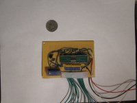
View attachment cad_bms_main.pdf
View attachment bom_bms_main.doc
So that's the perfboard "schematic" and resulting implementation for the main MAX11081 board. I've not gone to the effort of producing a 'proper' circuit schematic here, but it's pretty much the schematic on the MAX11081 datasheet with a few simplifications since I only needed fixed HVC/ LVC, didn't need to connect to adjacent modules and wasn't using the accompanying MAX11068 for balancing etc. The voltage of a few of the caps in the BOM might be a little higher than the Maxim datasheet/ perfboard "schematic" due to parts availability at Mouser.
I've implemented 3.5V HV cutoff and 2.2V LV cutoff. Not to everyone's taste, but easy to change.
The MAX11081 is in a tiny 38 pin 0.5mm TSSOP package, so I needed an adapter to get it to jive with 0.1" perfboard. I got a 40 pin adapter from EZ prototypes (they didn't have a 38 pin adapter for 0.5mm TSSOP). I had some trepidation soldering this tiny surface mount chip onto the adapter but it turned out to be about the easiest 38 pins I've ever soldered in my life! Judicious use of flux to prepare the adapter for soldering and then solder wick to clean up bridges made it a snap. I used a multimeter to check adjacent pins on the adapter weren't shorted and then ran one probe across the MAX11081 and the other probe across the adapter pins to verify that all pins had been connected.
A word of warning when buying the chip. I ordered from Mouser in November last year and they just e-mailed me last week with an updated estimated delivery sometime around the end of May this year. Yikes! I had a bad feeling this might happen, so I had ordered 3 of the chips directly from Maxim around the same time last November too, and they showed up a couple of weeks later. They were a few dollars more per chip, but I'm glad I did it now. I notice the companion chip to the MAX11081, the MAX11068, is "not recommended for new designs", which may mean the end is nigh for the MAX11081 too. Looks like they are being replaced by the tasty new MAX14920 and MAX14921 chips. Those behemoths don't look like good candidates for strapping to perfboard though.
I made a couple of schoolboy errors with the main board design that might be useful to know about.
o I initially powered SHDN from VAA. If I had read the datasheet thoroughly I would have realized that caused a chicken and egg situation since VAA isn't available until after a lengthy initialization process. IIRC the symptom of connecting SHDN to VAA was HV was not at the correct voltage above DCIN. So I changed the design so that SHDN tapped cell 1 directly to get it's 3V.
o I tried driving an optocoupler directly from ALRML. The spec sheet indicates a typical draw of 150uA from the pin, but doesn't indicate a maximum. However, it appears I got too greedy by going for 10mA! The punishment for this greed was that when an HVC or LVC condition occurred on a cell, ALRML would remain in the alarm state even after the HVC or LVC condition cleared. So I took a different approach, discussed in the section on the LVC board.
Throttle Pulldown (LVC)
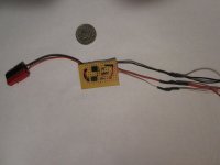
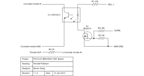
View attachment cad_charge_discharge_support.pdf
View attachment bom_throttle_pulldown.doc
As mentioned in the Main Board section, ALRML cannot provide enough current to drive an opto. So where do I get the necessary juice from? I considered 3 options:
1) Use a CR2032 cell on the LVC board to provide the power
2) Tap the first cell on the main board
3) Tap the first two cells on the main board
I rejected option 1) because the BMS was going to be buried inside my battery pack and I didn't want to have to worry about the condition of the CR2032 when charging/ discharging. Option 2) would work well with HVC, but with LVC, the voltage of the first cell could potentially be too low to effectively switch on a FET to drive the opto. So that led to option 3) - tap the first two cells. I didn't like the idea of two cells potentially being dragged to their death by a lengthy LVC condition though, so I came back to option 2) and found a few candidate low VGS threshold FETs.
My favorite was 2SK3019. It had a threshold between 0.8V and 1.5V. I knew it was small and my soldering skillz are limited, but I figured the triumph of will would overcome physical limitations. How wrong I was. I had tried to visualize the 1.6x0.8mm package by looking at the mm markings on my ruler, but nothing prepared me for how tiny they were when they landed on my desk. If you strapped one to a housefly it would look like a rowing boat on an aircraft carrier! I tried to solder one and it sucked itself onto the iron and disappeared inside a tiny molecule of solder never to be seen again. Then I sneezed and the rest disappeared into the shag pile. So I turned my attention away from sub-atomic devices and got some IRLD014. VGS threshold not as tasty, but much easier to work with for a homebrew project. In testing at 67F ambient, I found it pulled the throttle down strongly with the voltage of the first cell as low as 1.7V and still with some pulldown at 1.6V.
Note that the simple LVC circuit presented here relies on the alarm condition being cleared fairly quickly or the first cell could be drained to the point where damage occurs. Typically though, unless the user pushes through the alarm state, the cell voltage will recover sufficiently when load is removed to clear the alarm condition. It would have been nice if the MAX11081 provided some way of distinguishing LVC from other fault conditions too. As it is, if the alarm does not clear due to a cell being discharged so low that it does not bounce back, the charger disconnect circuit will also be disabled and the low cell will need to be brought up manually to 2.2V with a single cell charger, or perhaps charge briefly with the BMS disconnected.
Charger disconnect (HVC)
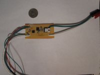
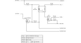
(perfboard layout is in previous section document cad_charge_discharge_support.pdf)
View attachment 4
When HVC was reached I wanted the charging process to stop and not kick back in again if cell voltages relaxed. To that end I used the optotriac circuit presented where resistances are set to ensure that once the triac is turned on then it remains on. When the optotriac is conducting, this effectively bypasses the 4.7K resistor between the power mosfet source and gate, and the gate is pulled close to ground and the power mosfet turns off.
This solution does depend on the charging device continuing to provide the requisite current and not detecting 'end of charge' and shutting off completely. There may be power supplies and chargers that will "drop out" at the low current level I have going through the triac via the 15K resistor. All I can say is I have tested the circuit with a Mastech HY10010E, a Meanwell NES-350-48 with Fechter current limiter V3 and a Soneil 36V 8A charger, and it functioned as required. It might be possible to get away with higher resistances than I used to minimize "wasted" power. The chosen triac will certainly remain latched with a much lower current. That said, with a 15K resistor, about 0.2W is wasted, so hopefully not too big a hit on the electricity bill or environmental conscience.
I used a Fairchild FDP5800 as the power mosfet. It's a logic level FET which isn't necessary, but it's what I happened to have on hand at the time. With suitable tweaking of resistors a cheaper non logic level FET, such as the Infineon IPP057N06N3 G, is likely to work just as well. I strapped a crude heatsink that was just a 1/2"x1/2"x1/4" block of aluminum to the FET and, charging at 10.2 amps in free air at ambient 69F found that the mosfet temperature stabilized at 105F as measured at the mosfet heatsink tab by an infrared thermometer (RadioShack 22-171 model).
The perfboard diagram ends up placing the FET upside down from what it should be. I only noticed that when I got to placing the transistor on the perfboard. I'll fix that in a future version and this will allow me to add a better clamped heatsink and get the operating temperature of the FET down a bit more, doh. Originally I had a two wire connection to the charger and the high voltage ground was permanently connected to the triac MT terminal. This worked for about a day, charging several times during that day, then it stopped working and the triac remained in a conducting state with the charger disconnected. Due to my limited electronics knowledge I had overlooked the fact that the body diode of the FET was allowing the battery to provide a current path for the triac with the charger disconnected. What's not clear to me is why the circuit worked for a day. I wouldn't have expected it to work at all. Anyways, to address the issue, I either had to implement an SSR with two FETs or add a third charging wire which would disconnect the triac when the charging cable was removed. I went for the latter, cheaper option.
Since there can never be too many different BMS implementations, I'd like to add a MAX11081 based one to the pile! At the time of writing, Googling for MAX11081 doesn't turn up much other than spec sheets, short news articles and a couple of short references of Endless Sphere, so hopefully this thread will add some useful info.
Motivation for the homebrew project: I've had bad experience with commercial BMS in the past. I was unlucky enough to purchase two that failed after a relatively short period of use. Manufacturer support was poor and it was looking like too complex a task to reverse engineer and fix them myself - I'm a software developer and have limited electronics knowledge, most of which has been picked up on the most excellent Endless Sphere.
I've used the wonderful Goodrum/ Fechter v2.6 BMS and it's been running reliably for several years in a bike now, and I've been following it's v4 development with keen interest, but I was looking for something simpler and cheaper again. What I wanted would be less feature rich of course, but would meet the basic requirements of providing LVC and HVC protection of cells and be simple enough to be built on perfboard - no need to get PCBs custom manufactured.
As far as cell balancing goes, I've had reasonable luck with cells staying in balance so I'll handle that with a cheap single cell charger and just do a manual balance every few thousand miles. Not a suitable strategy for everyone of course, particularly if cells of mixed ages and sources are used in a pack; in that case a more sophisticated BMS or more regular maintenance might be required.
It just so happened I wanted the BMS to work with a 36V LiFePo4 pack (fitted to this bicycle http://www.evalbum.com/4640), so the MAX11081 turned out to be a good fit since a single chip would handle all the cells for me. The MAX11081 doesn't need much in the way of additional components to do it's job either.
I ended up designing the BMS as a main MAX11081 board and two daughter boards, one for charger disconnect (HVC) and one for throttle pulldown (LVC). If I wanted to change HVC or LVC functionality, for example, to "go commando" and get rid of opto-isolation to save a dollar or two and live on the edge, then it was easy to just plug in the new design without touching the main board. As it is, the parts cost about $40 for the main board, including TSSOP adapter and perfboard, and about $6 total for the daughter boards.
Main Board

View attachment cad_bms_main.pdf
View attachment bom_bms_main.doc
So that's the perfboard "schematic" and resulting implementation for the main MAX11081 board. I've not gone to the effort of producing a 'proper' circuit schematic here, but it's pretty much the schematic on the MAX11081 datasheet with a few simplifications since I only needed fixed HVC/ LVC, didn't need to connect to adjacent modules and wasn't using the accompanying MAX11068 for balancing etc. The voltage of a few of the caps in the BOM might be a little higher than the Maxim datasheet/ perfboard "schematic" due to parts availability at Mouser.
I've implemented 3.5V HV cutoff and 2.2V LV cutoff. Not to everyone's taste, but easy to change.
The MAX11081 is in a tiny 38 pin 0.5mm TSSOP package, so I needed an adapter to get it to jive with 0.1" perfboard. I got a 40 pin adapter from EZ prototypes (they didn't have a 38 pin adapter for 0.5mm TSSOP). I had some trepidation soldering this tiny surface mount chip onto the adapter but it turned out to be about the easiest 38 pins I've ever soldered in my life! Judicious use of flux to prepare the adapter for soldering and then solder wick to clean up bridges made it a snap. I used a multimeter to check adjacent pins on the adapter weren't shorted and then ran one probe across the MAX11081 and the other probe across the adapter pins to verify that all pins had been connected.
A word of warning when buying the chip. I ordered from Mouser in November last year and they just e-mailed me last week with an updated estimated delivery sometime around the end of May this year. Yikes! I had a bad feeling this might happen, so I had ordered 3 of the chips directly from Maxim around the same time last November too, and they showed up a couple of weeks later. They were a few dollars more per chip, but I'm glad I did it now. I notice the companion chip to the MAX11081, the MAX11068, is "not recommended for new designs", which may mean the end is nigh for the MAX11081 too. Looks like they are being replaced by the tasty new MAX14920 and MAX14921 chips. Those behemoths don't look like good candidates for strapping to perfboard though.
I made a couple of schoolboy errors with the main board design that might be useful to know about.
o I initially powered SHDN from VAA. If I had read the datasheet thoroughly I would have realized that caused a chicken and egg situation since VAA isn't available until after a lengthy initialization process. IIRC the symptom of connecting SHDN to VAA was HV was not at the correct voltage above DCIN. So I changed the design so that SHDN tapped cell 1 directly to get it's 3V.
o I tried driving an optocoupler directly from ALRML. The spec sheet indicates a typical draw of 150uA from the pin, but doesn't indicate a maximum. However, it appears I got too greedy by going for 10mA! The punishment for this greed was that when an HVC or LVC condition occurred on a cell, ALRML would remain in the alarm state even after the HVC or LVC condition cleared. So I took a different approach, discussed in the section on the LVC board.
Throttle Pulldown (LVC)


View attachment cad_charge_discharge_support.pdf
View attachment bom_throttle_pulldown.doc
As mentioned in the Main Board section, ALRML cannot provide enough current to drive an opto. So where do I get the necessary juice from? I considered 3 options:
1) Use a CR2032 cell on the LVC board to provide the power
2) Tap the first cell on the main board
3) Tap the first two cells on the main board
I rejected option 1) because the BMS was going to be buried inside my battery pack and I didn't want to have to worry about the condition of the CR2032 when charging/ discharging. Option 2) would work well with HVC, but with LVC, the voltage of the first cell could potentially be too low to effectively switch on a FET to drive the opto. So that led to option 3) - tap the first two cells. I didn't like the idea of two cells potentially being dragged to their death by a lengthy LVC condition though, so I came back to option 2) and found a few candidate low VGS threshold FETs.
My favorite was 2SK3019. It had a threshold between 0.8V and 1.5V. I knew it was small and my soldering skillz are limited, but I figured the triumph of will would overcome physical limitations. How wrong I was. I had tried to visualize the 1.6x0.8mm package by looking at the mm markings on my ruler, but nothing prepared me for how tiny they were when they landed on my desk. If you strapped one to a housefly it would look like a rowing boat on an aircraft carrier! I tried to solder one and it sucked itself onto the iron and disappeared inside a tiny molecule of solder never to be seen again. Then I sneezed and the rest disappeared into the shag pile. So I turned my attention away from sub-atomic devices and got some IRLD014. VGS threshold not as tasty, but much easier to work with for a homebrew project. In testing at 67F ambient, I found it pulled the throttle down strongly with the voltage of the first cell as low as 1.7V and still with some pulldown at 1.6V.
Note that the simple LVC circuit presented here relies on the alarm condition being cleared fairly quickly or the first cell could be drained to the point where damage occurs. Typically though, unless the user pushes through the alarm state, the cell voltage will recover sufficiently when load is removed to clear the alarm condition. It would have been nice if the MAX11081 provided some way of distinguishing LVC from other fault conditions too. As it is, if the alarm does not clear due to a cell being discharged so low that it does not bounce back, the charger disconnect circuit will also be disabled and the low cell will need to be brought up manually to 2.2V with a single cell charger, or perhaps charge briefly with the BMS disconnected.
Charger disconnect (HVC)


(perfboard layout is in previous section document cad_charge_discharge_support.pdf)
View attachment 4
When HVC was reached I wanted the charging process to stop and not kick back in again if cell voltages relaxed. To that end I used the optotriac circuit presented where resistances are set to ensure that once the triac is turned on then it remains on. When the optotriac is conducting, this effectively bypasses the 4.7K resistor between the power mosfet source and gate, and the gate is pulled close to ground and the power mosfet turns off.
This solution does depend on the charging device continuing to provide the requisite current and not detecting 'end of charge' and shutting off completely. There may be power supplies and chargers that will "drop out" at the low current level I have going through the triac via the 15K resistor. All I can say is I have tested the circuit with a Mastech HY10010E, a Meanwell NES-350-48 with Fechter current limiter V3 and a Soneil 36V 8A charger, and it functioned as required. It might be possible to get away with higher resistances than I used to minimize "wasted" power. The chosen triac will certainly remain latched with a much lower current. That said, with a 15K resistor, about 0.2W is wasted, so hopefully not too big a hit on the electricity bill or environmental conscience.
I used a Fairchild FDP5800 as the power mosfet. It's a logic level FET which isn't necessary, but it's what I happened to have on hand at the time. With suitable tweaking of resistors a cheaper non logic level FET, such as the Infineon IPP057N06N3 G, is likely to work just as well. I strapped a crude heatsink that was just a 1/2"x1/2"x1/4" block of aluminum to the FET and, charging at 10.2 amps in free air at ambient 69F found that the mosfet temperature stabilized at 105F as measured at the mosfet heatsink tab by an infrared thermometer (RadioShack 22-171 model).
The perfboard diagram ends up placing the FET upside down from what it should be. I only noticed that when I got to placing the transistor on the perfboard. I'll fix that in a future version and this will allow me to add a better clamped heatsink and get the operating temperature of the FET down a bit more, doh. Originally I had a two wire connection to the charger and the high voltage ground was permanently connected to the triac MT terminal. This worked for about a day, charging several times during that day, then it stopped working and the triac remained in a conducting state with the charger disconnected. Due to my limited electronics knowledge I had overlooked the fact that the body diode of the FET was allowing the battery to provide a current path for the triac with the charger disconnected. What's not clear to me is why the circuit worked for a day. I wouldn't have expected it to work at all. Anyways, to address the issue, I either had to implement an SSR with two FETs or add a third charging wire which would disconnect the triac when the charging cable was removed. I went for the latter, cheaper option.

