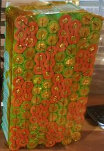
Currently remaking two 20s5p vtc6 packs I run in parallel to create 20s10p. (Removed all the original nickel strips to replace.)
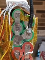
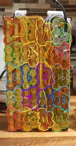
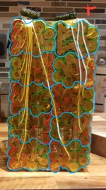
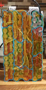
The pack is based around trapezoidal 5p groups all hot glued together, I could rearrange the pack but don't see the need unless someone tells me otherwise.
Plan is:
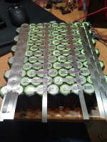
Series connections, triple layer 0.15*8mm full lengths. Parallel; single zig zag'd 0.15*8mm.
The packs should be capable of 150a pulse each with a continuous around 75-100a each.
I have a BMS's rated to 60a output each, but bypass them when I'm demanding big power.
The previous connections (about half inch of striped turnology 10awg high strand silicone insulated cable soldered over the last cell's nickel strip) didn't seem like they were up for the job.
Ill possibly go to 8 or 6awg next, but it's the attachment of said wire that has me uncertain.
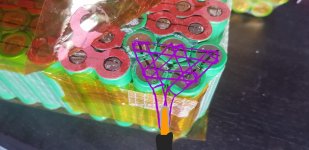
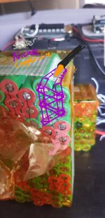
My current idea is to split the thick gauge wire and silver solder it to the nickel Strips across the 3 and 2 cell rows of the parallel group.
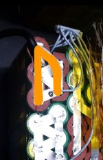
But I'm not fond of heating cells with a 80/100w soldering iron.
What other ways could I do it? Or better yet what's the best way of doing it?
The pack is based around trapezoidal 5p groups all hot glued together, I could rearrange the pack but don't see the need unless someone tells me otherwise.


Plan is:
Series connections, triple layer 0.15*8mm full lengths. Parallel; single zig zag'd 0.15*8mm.
The packs should be capable of 150a pulse each with a continuous around 75-100a each.
I have a BMS's rated to 60a output each, but bypass them when I'm demanding big power.
The previous connections (about half inch of striped turnology 10awg high strand silicone insulated cable soldered over the last cell's nickel strip) didn't seem like they were up for the job.
Ill possibly go to 8 or 6awg next, but it's the attachment of said wire that has me uncertain.
My current idea is to split the thick gauge wire and silver solder it to the nickel Strips across the 3 and 2 cell rows of the parallel group.

But I'm not fond of heating cells with a 80/100w soldering iron.
What other ways could I do it? Or better yet what's the best way of doing it?


