ZombieSS's power stage for Lebowski's controller video pg17

HighHopes said:
7.2V @ 90A with 60V switching right at 200nS.
take a moment to appreciate how difficult that is to obtain. let me say, not many can do that. great work so far, it is encouraging.

Is it good or hard to obtain?
So am I correct in saying my overshoot is only 7.2V based on how I have measured and compensating for the CMMR in the probes?

I can only take your word for it as I have VERY little experience in SMPS design, in fact this is my only experience with SMPS design, but I have done a tiny bit of hobbyist RF amp work to 450mhz before (no scope) and there are some parallels in design concepts.

I am also now second guessing my choice to use the boost stage as it appears it's much more than I really need, but time will tell the story on that. I have some IXYS 200V FETs that have a pretty big Qg.

How much of a difference would a set of differential probes make? Would it make my life easier and provide more accurate readings with less interference?

I found a set of Pintech 700V 100mhz differentials for $380 (I don't drink, smoke or gamble so buying educational things is my vice). I don't know the brand but I care little about brands if the specs are good and it works. It's not like I'm sending people into space or building medical equipment, I just would like something that does the job to the level I require.
Here is a link to the set with specs
http://www.pintech.com.cn/en/showpro.asp?id=1185&idc=1185&str=Differential%20Probe%20OEM

I am unfamiliar with differential probes but understand the concept of floating, I just modded 2 isolated power supplies to float from ground tonight by removing the earth ground reference which was tied to the neg output, I understand this is done for safety reasons, but I need pure floating goodness to put them in series and up my rail voltage! I have a pair of 120V:110V center tapped transformers which output something like 5A, they each weigh around 12lbs so I could rig up an isolation transformer (I have made one before this before with this pair) and float my entire scope, but that's a bit risky for my liking. Speaking of risky, while digging around tonight I found my HeNe power supply, I forget the specs but I know it's deadly. Bought it when I was 12 or 13yrs old to power a 5mW 632.8nm tube I use to have (I wonder what I did with my Michelson Interferometer I built in HS?).
 
I gave in and tested at 62V and then 95V tonight, I couldn't resist, here are the pics

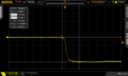
62V @ 95A, I was hitting the desaturation because my pulse width was too long and I didn't feel like reprogramming it until I went to 95V.
I am not doing a double pulse test yet, instead I have a pulse train triggering every 5 seconds with different pins having different time lengths. I'm working on coding up a decent single/double pulse generator which allows everything to be variable and has trigger intervals or is switchable to manual triggering.

What is the advantage of double pulse vs single pulse?

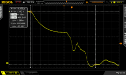
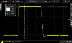
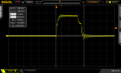
D-S on
d_s_on_62v_95a.png

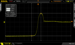
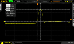
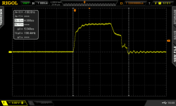
D-S off
d_s_off_62v_95a.png

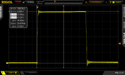
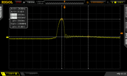
G-S pulse
g_s_62v_95a.png

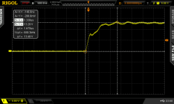
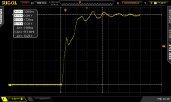
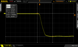
G-S on
g_s_on_62v_95a.png

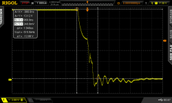
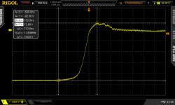
G-S off
g_s_off_62v_95a.png

High side Drain to Low side Source showing buss voltage, it's just a little higher than before, 13.2 - 5V correction for the probes = 8.2V of overshoot at 95A
hd_ls_62v_95a.png

These are at 95V buss 70-95A, 95A was it hitting desaturation. I shorted up the pulses to get data without desat triggering

D-S on 70A
d_s_95v_70a.png

D-S off 70A
d_s_off_95v_70a.png

G-S pulse 70A
g_s_95v_70a_all.png

G-S on 70A
g_s_on_95v_70a.png

G-S off 70A
g_s_off_95_v_70a.png

High side Draing to Low side Source 65A, corrected for CMMR it's about 7V overshoot
hd_ls_95v_65a.png

High side Draing to Low side Source 95A, corrected for CMMR it's 8.6V overshoot


In Summary, the driver/ MOSFET can:
Work at 95V/70A with a 260nS on 190nS off time, trigger desaturation protection at 95V/95A and the overshoot is only 8.6V @ 95V/95A

Just for the record, I have thoroughly tested the desaturation feature. This FET has over 300 pulses on it triggering the protection.

I scoped the low side MOSFET G-S under most of the above operating conditions, 95V/95A showed only a 0.7V rise on the gate pin of the MOSFET during turn on and a 4V spike during turn off which I do not believe is real because even with the low side gate shorted directly to the low side source it did not change. The low side looks clean to me. I also scoped and triggered the low side, it looks the same as the high side does, nothing stood out that made me take a screen shot to post here.

Next up is adding a second MOSFET and doing some more measuring. I'm surprised at how quickly the turn on/off times are with a single FET and 40 ohms worth of on/off resistors. I do not believe I need the boost stage, but I feel good knowing I know how to add it if needed. I hope HighHopes figures out how to implement it while keeping the 2 level turn off working.

Questions and comments welcome... should I simulate one or 2 pulses of a shoot through condition to the high side to see if it works? I'm pretty sure it will survive, but I realize 95V/95A is a lot to take. I would start off at 62V first.
 
double/vs. single pulse, the double is there so you can exercise the diode reverse recovery of the adjacent mosfet under load. your probes you do not have to see this, but it is the kind of stuff you look at when it is the first time you are using this mosfet and you need to qualify it for the application (some mosfets are better than others). obviously it like splitting hairs from DIY'er point of view, but sometimes it really matters a lot when you have challenging requirement. good luck meeting a mil-std radiated emissions with a snappy diode.. good luck.

the rounded hump you see on the D/S screenshots is probably not real. the peak voltage might be right, but that shape? i never seen anything like that. i must have done a double pulse test 10,000 times.. never seen that. but then i don't think i EVER used single ended probe for that either, so maybe that's what it would have looked like ;)

your switching waveforms look really really good considering the speed and that it is really stressed for one mosfet. i think its too fast but looks like the natural speed of the mosfet and your gate driver is not even breaking a sweat under those conditions.

when you add mosfets in parallel you may need to decrease your gate drive. i think you should target around 15 to 20 ohm. for this pulse testing you are really more looking at the gate driver side. how does hte power supply look when you add mosfets.. looking for excessive voltage droop during a pulse. so one mosfet has 15V and 3 mosfets has 12V? that's not good.. the most important thing to look at is the gate signal to detect any resonance/oscillation. well, the most important is current sharing but i dont think you have the proper tool to see that (you need a few very small regowski coils).

personally i wouldn't spend the money on the differential probe at this point. you don't seem to need to do any serious trouble shooting in this area and your design does not make critical use of the D/S voltage so you don't need to know precisely its characteristics, you don't have a stringent requirement to meet.. so.. why buy? but its your money. i'm just tossing my $0.02 in that's all.

definitely too risky to float your scope. i did it once and was lucky i didn't fry it, was an extreme situation.. i probably should not even mentioned it.

if i can give some advice. could be better to test 3-phase motor control at this point instead of pulse testing parallel mosfets. because right now you have one mosfet soldered in and know the performance of the drive. would be good to test all 3-phases with a quick pulse test each so you know the fault protection works on all drives, then ramp up a small motor with 10A phase current or so (something a single mosfet per switch can handle). then remove motor, short out the G/S of two phases and start pulse testing the remaining phase leg with 2, then 3, then 4 parallel mosfets. then install the mosfets in other phase legs (really no need to pulse test them) and try some real power testing. you see with the method described there is no discussion of having to de-solder any mosfets. if you parallel mosfet now and then later test for the first time 3-phase operation, you will probably have to remove mosfets so you risk only ONE during first time with 3-phase operation.
 
I need to place a small order with DigiKey now that I found the correct parts to use. I do not have enough parts to redo all 3 stages. At this point I think I am going to remove the boost stage from all the other drivers, I do not see it being needed since I want slower switching and I'm still at a whopping 40 ohms.

I'll monitor the gate drive power supply situation tonight. I want to solder in some parallel FETs and check the gate drive and also verify desaturation works as predicted, I have a feeling I might need to reduce my zener to a lower value, only real world testing will verify it and I want to make sure I get zeners in the correct range when I order my parts, I hate paying for shipping multiple times. I still need to modify 5 other drivers to be the same as this, then I will test each one quickly before moving on. Desoldering is easy, I have a Hakko 808 to harvest parts, fix MOSFETs in China controllers, etc. Super easy to remove through hole parts TO-220 devices take about 15 seconds. I think soldering tweezers or a hot air station are on the short list with all this SMD work I am doing.

If you say my waveforms look "really really good" then I'll hold off on the differential setup for now and add it to the wish list. The only one that concerned me was the D-S turn off with the funky hump/spike that doesn't match the ring freq and swings really far past ground. I don't think it's real, but I'm not 100%. Is there any way to verify it's false other than the fact you have never seen it before? I thought measuring the H Drain to L Source ruled out this as being false?

I posted several shots of my G-S at different voltage and current levels, they are a bit wavy, some of that is probably CMMR, but I do not see any crazy ringing. So would you give my G-S wave forms a passing grade for DIY application or is there anything else I need to be concerned about... I know I'll find out more with some parallel FETs.

What about when I run a motor, what should I look for? I'm going to have all kinds of noise going on and it's probably going to be a bit hard to tell what is real and what is not. The good news the motors I will be driving is 5x the inductance and 3x the resistance I have been using. I have noticed the higher the inductance the cleaner everything looks, even at the same current flow.

I checked out small Regowski coils a few days ago... ouch, those are expensive. Won't be getting one them any time soon.

P.S. I get the danger in floating a scope, I won't be doing that any time soon, I like my scope too much, plus a $4-500 probe is cheaper than a new scope!
 
Kids, don't try this at home with your cheap China controllers.

Dead short phase to ground, 62V, G-S 150A before it shut down! 7.3uS start to finish, just over 155A measured, 25uH 21mOhm load coil.
g_s_62v_150a.png

But you have to have faith that the system will support you... so man up and short the low side FET D-S and purposely create a 155A shoot through event, YIKES! Ok, this is just getting crazy to do this at 62V at 155A into a single IRFB4115 MOSFET, but I wanted to see if it would work and what the shut down time difference was (and if the FET would blow up). Surprisingly the FET took it gracefully. The FET shut was on and off in just 5.0uS! This is impressive, these devices (and this TD350E driver chip) is amazing!
I am purposely trying to blow up my FET and the gate driving is saying NO! Not on my watch you dumb ass!.
g_s_62v_150a_shootthrough.png
 
Parallel MOSFET testing is done.

Desat with 2 FETs is at 175A, with 3 FETs it should scale to about 230A, but that is off the scale of my current sensor. Tests were done at 62V with a 5uH coil.

D-S Turn on/off times for 2 FETs at 62V is about 230nS, with 3 FETs it goes to ~280nS. This is still with 40 ohm gate resistors. There is ZERO drop in the gate supply voltage. Looks like I have a go for light motor testing after I finish modding all my boards.
 
I have noticed the higher the inductance the cleaner everything looks, even at the same current flow.
inductor (or motor phase inductance) is a 1st order low pass filter for current. so, ya, gets cleaner as you go up in inductance.

dead short phase to ground, 62V, G-S 150A before it shut down!
wow... even i am impressed.

so man up and short the low side FET D-S and purposely create a 155A shoot through event,
ok, now you are just showing off. :lol:

when running 3-phase it is more a measurement of the control system than the power bridge. phase over current = soft shut down. it is nice to test other failure modes. i don't think you have protection for them but it is good to know what happens if you have open circuit phase cable (be careful of high voltage on open terminals). what happens if the DC bus collapses.. say normal is 100V, so what happens if it is 65V? if you do not have low voltage drop-out then what will happen? good to know these answers.

ps. i PM'd you a fix for the boost-stage + 2-step turn OFF. it was part of your design because we thought you might need it when you have 4 or 5 parallel mosfets.
 
I tested shoot through in 3 ways, with the 25uH coil, the 5uH coil and then dead short to ground through 1m of wire. A bit scary, but I had to know it worked and how quickly it reacted. I'm not going to tempt fate/injury and do a 100V test as I'm 99% sure it will work. If I am reading Fig2 and Fig 3 of the datasheet shows the FET was tested to 350A with up to a 60uS pulse with Tj=125C, but only at 50V. Specs say the FET is good for 420A pulses which is only limited by Tjc. I've monitored the buss and it's stays stiff during these events, only about a 1v drop if that since the pulse is so short. Since I know the driver reacts to this event in < 5.0uS I am calling it good to go and moving forward. This testing has been amazingly insightful.
 
just doing some more parallel testing real quick to double check.

Desat with a 5.6V zener in series with the 1.2V diode goes like this with parallel FETs, tests done with 5uH coil, 95V buss, 50uS commanded pulse.
The calculations showed I needed a 5.1V zener but bench testing proved I needed a higher one to reach my target around my desired over current point.

1 FET fault at ~90A @ 22c
2 FET fault at ~165A @ 22C
3 FET fault at ~250A @ 22C just barely off the max of the sensor
4 FET fault at ~325A @ 22C way off the scale so I estimated based on the curve.


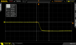
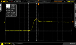
Here are some scope shots showing the D-S transition at 96V buss with a 30uS pulse and 4 FETs installed hitting desaturation protection which with 4 FETs is about 325A.

sensor appears to go to about +/- 240A, but that's beyond spec

Looks pretty nice, now I know I can go down on my gate resistors some.
D-S on of 625nS
d_s_on_95v_325a.png

D-S off of about 700nS
d_s_off_95v_325a.png
 
Compliments are more than deserved to this team that achieved successful implementation of deSat detection at 10 Kw levels! Incremental development and team collaboration in action! Well done guys!
 
bigmoose said:
Compliments are more than deserved to this team that achieved successful implementation of deSat detection at 10 Kw levels! Incremental development and team collaboration in action! Well done guy!

Thanks Dave! HighHopes offered to tutor me in his own proven method of design and I latched on, free education! I am absolutely amazed by the TD350E driver working so well, I know layout and component selection is one of the most critical parts and I would have never gotten this far on my own. This power stage was designed with all COTS hardware, no special parts such as non inductive resistors or trick parts like that. I think this entire 3 phase power stage has about $250 of parts in it including the PCBs which were $100 and I've already found some cheaper solutions for other parts.

If you look above you will see I tested desaturation with at least 325A through 4 parallel FETs at 95V. 31kW proven (untested in a shoot through test though, I figured a 5uH coil test was good enough. I am just not brave enough to do the shoot through test on my bench without a plexi shield and hearing protection, 99% sure it will work OK based on spec sheets and previous performance :) I don't think I ever would have thought of using desaturation protection without HighHopes making an informed hypothesis that it could work well for MOSFETs. I then got lucky and found another app note that described how to modify it's voltage level easily with a zener and the finished result is displayed above. You can probably tell by my enthusiastic posts I love this feature. If a setup can physically withstand me purposely trying to make it fail repeatedly 100s of times and working every time, then it should hopefully work in a real life situation that rarely occurs.

I think this design we (I hope HighHopes doesn't mind me saying we as he didn't want any credit if it didn't work :lol: ) came up with might be the first proof the concept can work with MOSFETs, not just IGBTs. I honestly don't 100% understand it's function in an FET. From what I am observing it's just measuring the shunt voltage of RDSon current generated by the MOSFET(s) during conduction then running through a comparator looking for > 7.2V, the TD350E fixed trigger point. I know there is an internal 250uA current that's in play somehow. I need to dissect the block diagram a bit and dig into it more. Just knowing it works and works well is good enough for me right now. 8)
 
"a little knowledge can be dangerous"

the desat protection is simple but powerful, its method of operation is somewhat bizzar. i remember the first time i tried to wrap my mind around it and was quite confused so you're not alone there! i'll see if i can brake it down a bit.

inside TD350 is a 7.2V threshold for the desat. whenevre the desat sense pin #14 reads a voltage greater than 7.2V then it triggers a fault. but where does this voltage come from?
firstly 7.2V is somewhat arbitrary.. they only need to pick a voltage that is higher than any mosfet D/S or IGBT C/E voltage that this chip is going to drive. the idea is that the high battery current that flows through the mosfet D/S, mulitiplied by the mosfet's Rds_ON = a voltage drop across the mosfet. it is THIS voltage that TD350 wants to measure but unfortunately you can't just take pin#14 and wire it direct to power mosfet D leg. the voltage is way too high. so, that is what component D7 job is.. to block the high voltage at mosfet D leg. conceptually, it makes sense to put D7 as first connecting to mosfet D leg because that is like you are saying "i want all high voltage blocked, not allowed in gate drive area" but when D8 is connected first to mosfet Leg as in your design that is like you're saying "well, i guess i'll let high votlage touch D8". this makes no sense to me, conceptually we do not want ANY part touching high voltage except those that are rated for it, and theoretically only the Mosfet and D7 are rated for it. but as you proved zombiess with your research. i was not immediately sold on your method to be honest, but your argument was sound so i .. grudgingly .. agreed. now you proved it on the bench so now i am happly agree with you (but still prefer my way :wink: ). anyway, so D7 blocks high voltage from entering gate drive circuit. D7 also has a voltage drop.. about 1.2V (see datasheet). now here is the important part.. D7 only has a voltage drop when current flows through it! obviously you see now this is what the TD350's 250uAmp current source is for. ha.. seems so simple now. immediately you see also that this is the same for D8. to reach a zener voltage there has to be current flowing through D8 too. so, when the 250uA flows through D8 then this part generates 5.1V. so we take D7 + D8 = 1.2V + 5.2V = 6.4V. does this voltage trigger the de-sat circuit? no.. desat threshold is 7.2V. now this 250uA, being dictated by kirkoff's current law, must return to its source (TD350) and the only path available to do that is through the power mosfet. so it flows through & returns to TD350. but along the way, wouldn't you know it, the power mosfet already has a voltage drop across it due to the high current flowing through the mosfet from the battery. for argument's sake, lets say that mosfet voltage drop is 2V for the amount of battery current flowing through it.

now.. desat trip:
D7 + D8 + Ids*Rds = ?
1.2V + 5.1V + 2V = 7.3V
is this voltage higher than TD350's desat threshold of 7.2V? yes it is.. so TD350 shuts down and issues trip flag.

** Note: let's say the mosfet's voltage drop was only 1V for same Ids current but you wanted TD350 to trip at same current (Ids = 200% FLA). only way to make this happen is to change the zener diode to a higher voltage part, like 6.1V. or, you could add in series another diode (two D7's).


ok.. so that is the principal of operation. but now you have to make it work in the real world.

Engineering = Theory + Application


how to make the application? firstly you have to understand 3 important things
1. D7 & D8 reached their full voltage at 250uA. you better readd some diode & zener datasheets to make sure you selected parts that actually CAN reach their forward voltage & zener voltage at so low a current!

2. this circuit success is directly tied to the voltage drop across power mosfet. you have to read the mosfet datasheet to understand a lot how current affects voltage drop

3. how does temperature change the voltages determined in item #1 & 2?

item #3 is super important.. you need to satisfy yourself that over the entire temperature range, all the variations in voltage, the TD350 will STILL trip for roughly the same current. this part is usually determined through analysis only, but you can hit your circuit & mosfet with a hair blower for 20minutes with a laser temp gun getting case temp... then test.
 
for the record.. the part that i was not sure would work is the voltage drop across the mosfet. i was concerned that the voltage would be too low to reliably pick up in a desat circuit we have here. votlage drop in a mosfet is exactly the conduction losses so manufacturers go way out of their way to make sure this voltage is low low low. its not the same in an IGBT as voltage across the device is not related to conduction losses in the same way so manufacturers relax and allow IGBTs to have much higher collector/emitter voltage (which is handy for detection in desat circuit).

i did have a backup solution in mind incase this didn't work for a mosfet.. but i really wanted zombiess to prove this out because the method is elegant.. and cheap :mrgreen:

so the only thing left to show for success of this desat scheme is to know your analysis (math) will determine desat will work over the operating temp range. i'll leave that for you to ponder :?:
 
HighHopes said:
so the only thing left to show for success of this desat scheme is to know your analysis (math) will determine desat will work over the operating temp range. i'll leave that for you to ponder :?:

Putting D8 after D7 was a decision made based on an app note. Avego 5324 to be exact, I just found it and it even mentions using it with MOSFETs.

You say the D8 zener is touching high voltage, is it really? The only current path it can take is from desat out to the driver ground, correct? With the MOSFET in it's non conducting state there is no path to ground available so it has +Vbatt on it with reference to -Vbatt, but there is no current path to get to -Vbatt without a fault, correct? Under what condition would the zener flow current from +vbatt into pin 14? None that I know of as long as D7 is in place and functional. We don't worry about the +Vbatt touching the GND of the TD350E driver when the MOSFET conducts do we? Nope, there is no current path available.

Only when the MOSFET conducts is current able to flow through and complete the circuit, so why does having a zener diode on the B+ or phase really matter? Is it breaking a design rule? Does that rule actually apply in this case? I understand your argument that D7 block the voltage and should be first, but it's just is the same even if there is a zener there, only allow current to flow in one direction, Desat -> power device -> driver ground. If you were running at full speed towards a door and just as you get to the door someone opens it for you, but right behind that door is a wall... Same scenario but there is a door behind the wall, you are still running full speed to get to the door, but this time you never make it to the door because someone put a wall in front of it, same outcome.

As for the thermal issue we know that FETs RDSon resistance increases with temperature, I think you know I know this, but I'll type it out anyways for everyone else who stumbles upon this. This is in fact a very desirable effect for the desaturation circuit as it acts as an automated derating system. Higher resistance = more voltage drop on the desaturation circuit = triggering at a lower current.

I have a spreadsheet that automatically calculates the RDSon and Desat voltage based on the MOSFET Tj.
My target of 50A RMS for an MOSFET with 25% peak overcurrent comes out to about 88A at 25C for an IRFB4115 with a 10ohm RDSon. AT 125C Tj the desat circuit crosses the 7.2V threshold at just 44A peak, a 50% reduction in current. Fig 8 and 9 of the datasheet show it's current capabilities for different Tj and Tc conditions.
Of course this means the opposite is true, when it's colder, say 0C the amount of current allowed before desat triggers is higher. I calculated at 0C Tj the current to trigger desat will be about 129A which is still within as single devices pulse rating (I have shown on the bench how fast the circuit reacts, <5uS).

The other concern is paralleling MOSFETs. The math and more importantly bench testing has no real effect on the desat circuit other than upping the allowed current before fault. This is good as we do not need to compensate as we parallel for higher power, it's built into the system due to the RDSon becoming 1/(1/R1 + 1/1Rn) My testing shows that this holds pretty close to reality and is predictable.

I realize that when choosing MOSFETs all these factors need to be taken into consideration.

Thank you for the explanation of the desat circuit, it now makes perfect sense on how it works. Feel free to tear apart my D7/D8 scenario, but I believe I am correct, and I copied it from the Avego engineers so if I'm wrong to put it first, then so are they. :lol:

BTW, looking at that app note I just noticed they talk about false fault detection prevention from reverse recovery spikes from the freewheeling side pull the desat pin below ground and they show a fix for it using a schottky diode and another zener. I have not seen any false triggering in any of my tests so I believe I am in the clear. I have been testing with some very low inductance loads, all the way to dead short.
 
Thanks for sharing that highhopes.
So the desat detection can be done with the ir2113 driver just not as elegantly I say this because I was always wondering why the SD pin was put high to shut the Driver down... Maybe they did this on purpose and maybe there is a patent on the term desaturation detection so IR just put it in their driver knowing it would be used in this same way if needed.???
 
nothing electrically wrong with placement of D8 (it would be smoke by now if there were), just conceptually it is odd .. to me. i like it when things make sense, then i feel like i can understand it better which is important to me.

I have a spreadsheet that automatically calculates the RDSon and Desat voltage based on the MOSFET Tj.
perfect, now add also the temperature affects of D7 & D8 and threshold voltage of TD350. then look at the range of current you can expect Desat to trigger in. too low and it will trigger within your normal operating current, too high and risk over stressing mosfet(s) or DC link cap can't hold the bus (not an issue in your current design). its a pretty big range, so you can see desat is not particularily accurate, but it doesn't have to be, it need only be reliable.

This is good as we do not need to compensate as we parallel for higher power, it's built into the system due to the RDSon becoming 1/(1/R1 + 1/1Rn)
i was thinking about this early this morning, what the effect of paralleling mosfets would be on desat. first i was thinking if i put two mosfet's in parallel it is because i want to double the current but i have 1/2 the resistance now so the voltage drop is the same and so desat trigger at exact same level as when i had just one mosfet. but .. Engineering = theory + application.. so i think more about the application in real world. when i put two mosfets in parallel do i really get double the current? no, and i don't need to tell you that as you are the expert on parallel operation. what you find is that the mosfets do not share current equally so as a result you have to keep some safety margin (less margin if you make an effort to match mosfets). for example, one mosfet is good for 35A then two is NOT good for 70A, but only 65A (just an example, not real numbers). so for two parallel mosfets actually there is slightly less current than "double" and so slightly less voltage drop and thus the desat threshold voltage will be too high (theoretically). thankfully, the range of operation of the desat circuit is huge, and the voltage threshold change is small (especially when you match mosfets) so no issue here at all which was exactly your feeling from the beginning ( i just put a lot of unnecessary words beside it).

BTW, looking at that app note I just noticed they talk about false fault detection prevention from reverse recovery spikes
ya that's a real thing but TD350 people already know of this and put two features to help compensate.
1. there is a low pass filter to help with "noise" R17, C11.
2. there is a "blanking time" which basically means the desat circuit is disabled while waiting for the Mosfet to finish the turn ON process and settle out, so the circuit is disabled when there is a lot of noise.

arlo:
So the desat detection can be done with the ir2113 driver
yes... and no. the circuit can be added, but, you must have two additional things.
1. a blanking time
2. disable mosfet (and soon after all other mosfets) if de-sat is triggered.

interestingly, when you someday decide to design for your high switching frequency you want, this story will be told in full. because there is no gate driver on the market today that has a built in desat function which is also capable of switching >30kHz. so the desat circuit which must be present in designs >1kW (in my opinion) has to be implemented using discrete parts. i.e., you have to design a blanking time. and.. to make things interesting, any circuit you design has to be done very carefully because the gate driver is critical application in a high noise environment with a bouncing ground reference.. not easy! but it will become easy once we start talking about it and working the details. all in good time. :)
 
Maybe this desat scheme was born in this paper here?

http://www.tf.uni-kiel.de/etit/LEA-download/dl-open/veroeff_2010/wittig_epe_pemc_2010.pdf

Zomb, just look at how "similar" it is to yours, the Vds turn-off behavior on their tests.
 
Njay said:
Maybe this desat scheme was born in this paper here?

http://www.tf.uni-kiel.de/etech/LEA/dl-open/veroeff_2010/wittig_epe_pemc_2010.pdf

Zomb, just look at how "similar" it is to yours, the Vds turn-off behavior on their tests.

The resemblance is remarkable, but is it a function of the desat or the probes? Either way it is a great arrival which shows how to do desat with descrete components. That's going in my notes for future reference. Anyone want an ixys 8 or 14a driver with low propagation delay and desaturation detection?

2 level turn off done discretely anyone?

Fun for another day. I can only slay one dragon at a time and right now I still have a ways to go on this quest. I have started a new td350 layout which is all SMD to reduce the driver foot print. It looks good to me so far but I am still new to proper layout.
 
Not to rain on anyone's parade or anything... but what the desat detection does as far
as I understand is switch off a FET when the other one has blown and is conducting.
So it protects the remaining FET, just like a simple fuse.
It will not prevent the first FET from blowing up ...
 
Anyone want an ixys 8 or 14a driver with low propagation delay and desaturation detection?
and that my friends is EXACTLY how to do a high frequency gate drive for low inductance machine (you stole my thunder Njay, you're too good! lol). now read the paper carefully and make sure it has some sort of blanking time and fault output.

lewbowski:
off a FET when the other one has blown and is conducting
the beauty of the desat circuit is that it shuts off the mosfet DURING a fault and BEFORE it (or any other mosfet) gets damaged; if that were not true zombiess would have had a fire for sure with his aggressive testing. so it is completely saved for operation again after a brief cool down (well, better you find out what caused the problem before going again, but at least you have options without waste of money). i suppose you could argue that each time a mosfet survives a shoot-through a portion of its lifespan is reduced.. so instead of lasting 20 years, now it will last 19 yrs 200 days or something like that.


ps. the desat circuit zombiess is using is atleast 14 years old because it was well understood before i started working in the field
 
oh neat.. just reading that paper now and look at figure 8. see the green D/S waveform with the rounded hump. look familiar?
 
just a quick note.. on high frequency gate drive you can not use 2-step turn-OFF because it takes too long. it is like a 1us propegation delay waiting for mosfet to turn OFF. nice feature for a DIY gate drive for use at 20kHz though. so you have to dream up some other solution to manage the mosfet D/S voltage spike that occurs after shut-down during a high current fault. hint.. see my gate drive schematic in different forumn ;)
 
Lebowski said:
Not to rain on anyone's parade or anything... but what the desat detection does as far
as I understand is switch off a FET when the other one has blown and is conducting.
So it protects the remaining FET, just like a simple fuse.
It will not prevent the first FET from blowing up ...

As HighHopes stated it saves the FET that is faulting. I have proven this without any doubt by purposely creating a shoot through condition and shorting my low side D-S together so the high side MOSFET has to absorb all the energy. My single IRFB4115 FET survived at least 20 events of 64V 155A and it still works fine. The event is detected and the the FET turned completely off in under 5uS, the 5uS is the gate charge going from 0V-13V-0V so the FET is only on for maybe 3-4uS This is well within the FETs pulse rating spec which is 420A, Tj limited@175C. The datasheet shows it was tested at 50V 420A pulses for up to 60uS at it's pulse rating at 25C.

Without this circuit I'm pretty sure dumping 4mF charged to 64V with a 3A power supply still connected into a shorted FET with only 1M of uncoiled wire acting as an inductor would cause a nice little explosion on my work bench after the first pulse.
 
HighHopes said:
just a quick note.. on high frequency gate drive you can not use 2-step turn-OFF because it takes too long. it is like a 1us propegation delay waiting for mosfet to turn OFF. nice feature for a DIY gate drive for use at 20kHz though. so you have to dream up some other solution to manage the mosfet D/S voltage spike that occurs after shut-down during a high current fault. hint.. see my gate drive schematic in different forumn ;)

Is that what those other diodes are doing that I don't quite understand in your schematic?
 
zombiess said:
The resemblance is remarkable, but is it a function of the desat or the probes?
It means is just real.

I had never seen the rounded hump before, but my experience is very reduced. Maybe something to do with the very fast current switching. It's like the diode took some time to turn on, then when it did it drastically reduced the voltage raise creating the hump. I don't know, but looks like bad news because the overshoot is just huge.

HighHopes said:
(you stole my thunder Njay, you're too good! lol).
lol, I wish!!...


Update: I did some simulations, I can see the hump. It's around and beyond 100A and with the compliments of the parasitic inductance between the 2 FETs (of the half-bridge). This inductance is probably making it difficult for the current to change path from one MOSFET into the diode on the other.
 
Back
Top