ZombieSS's power stage for Lebowski's controller video pg17

Njay said:
zombiess said:
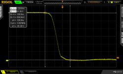
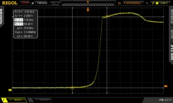
The resemblance is remarkable, but is it a function of the desat or the probes?
It means is just real.

I had never seen the rounded hump before, but my experience is very reduced. Maybe something to do with the very fast current switching. It's like the diode took some time to turn on, then when it did it drastically reduced the voltage raise creating the hump. I don't know, but looks like bad news because the overshoot is just huge.

HighHopes said:
(you stole my thunder Njay, you're too good! lol).
lol, I wish!!...

Check out my single FET D-S at 70A 96V and then the very last pic I posted of 4 parallel FETs at 325A 96V. With just one FET the mystery hump is coming in at 124V. With 4 parallel and 5x the current flow the hump is only 104V. The switching is much slower on the 4 parallel FETs, so I need to determine if the size of that hump is being controlled by the paralleling of the FETs or the switching speed. I did notice that if I kept my current flow around 70a and added FETs in parallel the hump reduced and the small amount of ringing completely disappeared. The ringing frequency got lower as FETs were added.

Even if the hump is real, it's not a percentage of the buss as it appeared. At 104V it's very manageable. I would like to be able to max out the voltage on this controller at 125V, but I'm not sure if that will happen, it does look like it will be successful at 100V buss which is my main target. Once I change gate resistors I'll be able to see if that spike/hump is switching speed related.
 
You missed my update:
I did some simulations, I can see the hump. It's around and beyond 100A and with the compliments of the parasitic inductance between the 2 FETs (of the half-bridge). This inductance is probably making it difficult for the current to change path from one MOSFET into the diode on the other.

In your 1 vs 4 parallel I think the hump reduced due to reduced switching speed. I can see that in the sims, if I increase switching time it will of course be smaller, but it is still there (current is kept at the same value).

So switching time and parasitic inductance between both top and bottom FETs look like the main inputs for the hump height at a certain current.
 
Njay said:
You missed my update:
I did some simulations, I can see the hump. It's around and beyond 100A and with the compliments of the parasitic inductance between the 2 FETs (of the half-bridge). This inductance is probably making it difficult for the current to change path from one MOSFET into the diode on the other.

In your 1 vs 4 parallel I think the hump reduced due to reduced switching speed. I can see that in the sims, if I increase switching time it will of course be smaller, but it is still there (current is kept at the same value).

So switching time and parasitic inductance between both top and bottom FETs look like the main inputs for the hump height at a certain current.

Yes, I missed that. What happens to the hump when you up the voltage or increase the inductance between the FETs?

What are you simulating with? I'm new to simulating analog circuits, just got my hands on Cadence PSpice, it's going to be a steep learning curve. I also have access to Multisim 12.0. Current distance between my two installed FETs is 54mm center to center.
 
NJay, can you post your simulation circuit?
 
Sure, here it is, pic and "source" (LTspice).
Note also that (not visible in the pic below) the lower frequency ringing that can be seen at turn off after the high frequency ringing is caused by not enough DC-link capacitance, that is, it's probably resonating with the wiring inductance (the 500uF need to go to 1500uF to attenuate the ripple to 2V over Vbat)

8g7w.png
 

Attachments

  • turn-off-hump.zip
    330 bytes · Views: 26
Just a quick update. HighHopes came up with a mod to get the 2 level turn off working with the boost stage and I verified it works in hardware. It's actually the same as seen in the TD350E app note on adding a boost stage (neither of us had seen it done that way before). When using the boost stage it requires a diode to use a separate turn off resistor if you want to use separate ones in your design. Personally I find the TD350E is outputting enough current for this application so I am going to remove the boost stage. If I want to drive more than 3 IRFP4568's in parallel, I might require it due to the amount of gate charge they have. I am actually surprised at how little power is require to switch quickly. 95V in 620nS with a minimum of 308nC Qg total for all 4 and this is with a 40 ohm gate resistor, so it has the capabilities of switching much faster. Keep in mind this is only a 1.5A driver so it's not particularly powerful. Now I have a better feel for how much gate drive current is going to be required for a design criteria.
 
Another interesting scope shot post.

In this post I tried HighHopes reccomendation to add a small G-S capacitor on top of the G-S resistor I am using. I tried a 15nF and a 47nF, below are the results.

Shots were taken on the high side FET with 24V buss, 50A discharge into a 25uH coil.

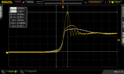
First up, a comparison shot of all 3, 0nF vs 15nF vs 47nF, At 0nF my switching time is 150nS with a big spike and some ring after the massive overshoot.
g_s_24v_50a_0nf_15nf_vs_47nf.png

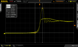
0nF vs 47nF. You can see the 47nF really calms things down, the switching time goes to 320nS from now much lower peak, sorry, lost the other reference shot with the proper overlay so both are yellow traces, 0nF is the active one.
g_s_24v_50a_0nf_vs_47nf.png

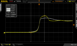
15nF vs 47nF, switching time goes to 280nS and it has a bit more overshoot than the 47nF. Just adding this single 15nF cap reduces the overshoot from 26V down to just 11V and that's without correcting for the CMMR the probes have which is around 4V at this current / buss voltage.
g_s_24v_50a_15nf_vs_47nf.png

I have noticed similar results as I start to parallel the FETs, but even then it's still not this good.
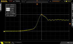
Here is 4 FETs in parallel, same settings, no caps. 470nS switch time and still has a 12V overshoot which is still 1V higher than the 15nF cap
g_s_24v_50a_4parallel.png

So adding a 15nF cap on top of the G-S resistor really reduces the overshoot and neutralizes the small amount of ring while adding 130nS to the switching time of a single FET. I am guessing it might help by neutralizing some of the parasitic inductance between the G-S resistor because the ring frequency really changes to a much lower one and a much lower amplitude. Ringing is caused by parasitic tank circuits, correct? If so then adding capacitance helps to neutralize any parasitic inductance that exists between the G-S and also the larger C value would cause the frequency to shift lower. Compared to 4 FETs in parallel, the frequency shifts lower, by only by around half, not the order magnitude the G-S 15nF cap is providing. I noticed slower switching speeds reduced the initial peak, but paralleling 4 FETs which slows down the switching time shows a much different result from just adding a single simple G-S capacitor.

Thoughts anyone? Is it OK to run a 15nF cap G-S in a production drive? I am thinking I can use the 15nF caps and reduce my gate resistor to get my switching times quicker and have even better results.
 
New zener diodes installed for the Desat, I went with 5.6V again, but this time they are really close on the actual zener rating because I verified the current on the datasheet before selecting them and they are around 5.3v at 250uA. I checked it with 3 FETs and it's trigging right around 210A which is just about right, with 4 that gives me a fault at 280A peak This is significantly less than the other 5.6V zeners I had installed temporarily. Just goes to show there is no substitute for bench testing. One FET was triggering at ~70A. With the other 5.6 zener I had installed it was getting to almost 90A per FET before faulting. Faulting at 280A peak means I can get to 198A RMS, if I was using a sensor with enough range +/- 300A vs the +/- 200A sensor I am using now.

I also tested the fault output signal. During normal operation the signal is held high at the opto output. When a fault occurs the line drops to 0V which I am using a PIC to detect. It stays at 0V until the next cycle comes through which resets it. Having my PIC detect and shut down the other outputs is will need to be done quickly. I'll probably use an interrupt or a really tight loop that polls the fault pins. I have a diagnostic LED on the board which I plan to have blink out error codes to me when a fault occurs so I know what phase and high/low side caused the issue.

I'm in the process of making all the changes to the boards so that I can run a motor next... Finally!
 
zombiess, this is great stuff. So simply adding a capacitor parallel with the gate resistor can help reduce ringing on the FET gate, is that correct understood?

I haven't been able to find the basic explanation of what a desat circuit really is but I have been reading your posts here and could you please tell my if I got it wrong?
What I understand: Some circuit is monitoring the voltage drop across the drain-source of the FET. If this voltage reaches a certain level, too much current is passing through the FET and the desat circuit tells the gate driver to pull the gate low to turn off the FET. Your gate driver has some built-in feature for this, but if the driver does not have this feature, how is this done then? Some comparator that is connected to the gate driver input?

Does the desat circuit have to monitor both the high side FETs and the low side FETs or is it enough to monitor the low side?
 
Futterama said:
zombiess, this is great stuff. So simply adding a capacitor parallel with the gate resistor can help reduce ringing on the FET gate, is that correct understood?

no, it is parallel to the discharge resistor beteween the gate and source.

so it will form a lowpass filter with the gate resistor and the two resistors.
 
speedmd said:
If I am not mistaken, it will be a band pass filter when in parallel with the resistor.
Its parallel to a resistor with a high value 5-10k usaly its the pull down resistor both the cap and resistor are from gate to source so the cap is adding some cpacatance to the amount the driver is feeding (capacatance of the gate charge).
 
nieles said:
so it will form a lowpass filter with the gate resistor and the two resistors.

According to what I just read a parallel RC filter only works when it's feed by a current source because Vin=Vout, but I do not understand exactly what it is doing in this circuit beyond slowing down the gate rise/fall time because it's acting as additional miller capacitance (I think). I suspect the cap is helping to cancel out some of the parasitic inductance induced effects that exists in the traces connecting the 4.7k the G-S resistor since the ringing frequency changes dramatically (with out it, the little bit of ringing is in the +20mhz region, but low in amplitude so I'm not concerned about it) vs just slowing down the G-S switching time. HighHopes has a more solid understanding of what this cap does. I have googled it and not found much info, but the scope pictures sure look pretty! Adding the cap certainly changes the resonating frequency a lot.

Gate drive theory + real world testing = welcome to the jungle, we got fun and games!
 
Is it OK to run a 15nF cap G-S in a production drive? I am thinking I can use the 15nF caps and reduce my gate resistor to get my switching times quicker and have even better results.
yes perfectly fine, in fact it is part of my default design but i add it as a "do not populate" part so its added only if needed. adding cap has benefit but also negative.. power supply requirement goes up, mosfet speed of switching goes down (can be a good thing) and mosfet losses go up (can be tolerable, can exceed your limit) so keep an eye on it.

adding a cap G/S is like adding a low-pass filter. in reality, the very low gate resistance and extremely small cap value makes the low-pass filter's cut-off freequency quite high, like 500kHz or something. which parts of the gate drive ON/OFF commands are of that frequency? only the very very edge of the PWM signal. everything else is less frequency so no filtering on that. but it is enough just to softly damping the sharp edge of the PWM signal. in fact you get the same effect by adding parallel mosfets because each mosfet is like adding a small capacitance for the low-pass filter (this was shown by zombiess recent posts). but there is a very subtle difference when you add an external cap.. what you are adding is a PURE capacitor (so to speak) as compared to a mosfet gate input which is an "effective" capacitance. so the external cap will take that first punch of current from the gate drive IC because it is a pure cap and THEN then mosfets receive their charge. internal to the mosfet is a lot of physics, moving of electrons, biasing this junction and that junction.. when you smooth the current who's job it is to energize the mosfet gate then this allows mosfet to be charged in a much more smooth fashion which is evidenced by a nice switch D/S.
 
HighHopes, I have a question about the G-S caps. So I am planning to run up to 4 MOSFETs in parallel, should each one have it's own G-S cap, or is only one needed for the entire system? I have four 4.7k resistors on each high/low side, but right now I only have 1 FET and 1 15nF cap installed for each. Since the other G-S resistors are populated and all G-S connections are paralleled the effective G-S resistance is around 1.17k, four 4.7k resistors in parallel. If 15nF works good for 1 MOSFET, would it be good to scale up and use four 4nF caps when I have 4 MOSFETs installed totally 16nF? I don't think a 15nF per MOSFET is really needed, that would end up giving my 60nF capacitance which would really slow down the switch times.

What is the best practice in this situation? I am thinking it's more logical to have 1 per MOSFET and have the sum of them in parallel equal the required capacitance to achieve the desired wave form. I have a pretty good feeling that with some experimenting here I can get a low gate resistor (I am now at 20 ohms, down from 40), cleaner wave form edges and quick switching times.

All 3 boards are built the same now, just need to bench test each with the pulse setup before I try and hook it all up to the controller and spin a motor.
 
i do not know the answer to that question, paralleling mosfets in your design was a first for me. glad to practice on your boards though ;)

i would be inclined to put just one pull-down resistor and one G/S cap because it is cheaper, less board space, but most important all mosfets will have same performance from this single cap influence (i.e. tolerance of this cap will be the same for all mosfets) and the critical part - synchronized switching - will hopefully be better controlled.
 
Zombies I usually do something like that as a one per fet item. I do this for better balance as in trying to keep things equal. But depending on your design that might not matter.
I usually run a separate pull down per fet and separate zener on each fet gate too. Its hard to say what happens in a little distance on a trace so I trust having the safety components as close to each fet at possible.
 
I'm bench testing the boards right now. Gate resistors are 20 ohms, I have a single 15nF G-S cap soldered on top.

So here is another question about paralleling. I am using 4.7k G-S resistors to hold the gate state low so I always know my state. Should I only be using a single 4.7k for all my paralleled MOSFETS or is it better to use 4 of them and let the G-S resistance drop down to 1.17k? I am thinking I really only need a single resistor and cap, that could make my new board layout much cleaner if I get rid of all but one of them, not to mention a lower parts count.

BTW, 20 ohms gate resistor + 15nF cap G-S = 150nS switching times. I'm thinking I should bump it up to around 30nF. It really helps with that funky spike overshoot. Even at lower buss voltage where the spike is usually 2x my buss voltage, it's now much lower. I'm running 36V buss for testing right now which would normally cause the overshoot peak to be around 30-36V at 150nS switch times and it's only 12V (not corrected for CMMR), that's a huge difference for just a tiny cap. A larger cap will reduce it even further, so will paralleled FETs.

Arlo1, are you using zeners to try and protect the gate from a Vgs spike? You can probably eliminate it in your next design if you go isolated supplies. I don't have any protection on my gate input.
 
All driver boards are now tested and passed. The current sensor was also relocated to the bottom side to fix the polarity issue.

I should hopefully be able to spin a motor tomorrow if all goes well. I'm 90% sure I want to increase the G-S cap to 47nF or even higher to slow down the switching time, 150nS is seems too quick to start off at with a motor, but the CMMR corrected overshoot at turn off is only about 6-7V and 15V on a dead short 150A fault at 62V.

I think for the first test I'd like to have my switching time at >=500nS and work from there. That G-S cap is like magic to fix my overshoot spike and kill off the small amount of ringing. I'm also thinking I should probably remove the other G-S resistors since I only need one.
 
So I made one last round of changes because I wanted to tweak this a little more before firing everything up with a real load. I removed the other 4.7k G-S resistors so that each side only has one. I left the 15nF cap G-S cap installed and added an additions 47nF cap for a total of 62nF G-S capacitance. This slowed my switch times down to 325nS at 62v with 75A going through the load coil, it also cleaned up the overshoot even more, only 10v as displayed.

325nS turn on time
g_s_on_62v_75a_62nF.png

325nS turn off and a much cleaner result
View attachment 1

325nS tun off
g_s_off2_62v_75a_62nF.png

I'll mod the other 2 boards tomorrow so that I can finally get them hooked up to the controller board and hopefully communicating / turning a motor in the next day or 2.

Driver circuits are drawing 15.5mA each at idle and under 19khz switching go up to 25mA each which is 50% of the isolated supplies input current. Adding the capacitors has increased the power demand on the isolated supply, but only by a small amount.
 
67nF is pretty large for G/S smoothing cap. keep an eye on your mosfet case temp when operating with motor to see if switching is too slow.
probably better to wait until you have differential probes before you make conclusions about D/S waveforms.

remember to when you put current sensor on the bottom side to make sure the sensor power, ground & signal connections line up correct to your PCB layout.

looking forward to seeing your 3-phase test run.
 
HighHopes said:
67nF is pretty large for G/S smoothing cap. keep an eye on your mosfet case temp when operating with motor to see if switching is too slow.
probably better to wait until you have differential probes before you make conclusions about D/S waveforms.

remember to when you put current sensor on the bottom side to make sure the sensor power, ground & signal connections line up correct to your PCB layout.

looking forward to seeing your 3-phase test run.

1st of 2 differential probes arrived today. I am reading the manual now. Need to go grab a 50 ohm terminator and BNC t for it right now. Last calibration on it was done in 1996. Probe is probably from the 70s or early 80s. It came with all accessories too. Total cost $180 and its a Tek.
 
Everything is now hooked up, serial communication established to the brain board. I should be able to test a motor tomorrow. I have already done a PWM test to verify the driver boards are receiving signals and working.
 
Following you and arlos's posts on controller design and testing is like learning to appreciate opera, I might not understand half of what's being said, but I can't help but become caught up in the music! Good luck!
 
hal2000 said:
Following you and arlos's posts on controller design and testing is like learning to appreciate opera, I might not understand half of what's being said, but I can't help but become caught up in the music! Good luck!

You have to start somewhere and learning power stage design is like eating an elephant while painting a Jackson Pollock. Eating is done one bite at a time, go slow, it's also good to have a teacher, read as many manufacturers app notes and understand them. That usually means downloading an app note, then looking up app notes on things you read about in the app note so you can understand what it's talking about :lol: The actual design/layout is like a Jackson Pollock painting, you have to capture the chaos and then frame it. It's as much science as it is art, extremely helpful to have a "master" give you an apprenticeship on this one, but that is easier said than done. If you do find a master, do it his way first as it's already been proven; don't try to improve on his work until you understand how and why it works. This last one is where I've seen most of people go wrong. I've studied several subjects under different "masters" and did it their way until I could offer my own input and then justify my reasoning. I also have some experience being the master and offering up free information and even entire systems to copy, but I've never had anyone actually "copy" something that I proved was 100%, they always had to "improve" on it, usually failing to some degree or completely in the process.

Don't be afraid to fail, you still learn. It's not a failure, it's just an undesirable possible outcome. :mrgreen:
 
Back
Top