• Hello ES! We could use some help to get us past the finish line on building the new knowledgebase for the forum.
    Can you donate? Please see our fundraising page. Thank you!

3Kw Charger with Balance Project

Mihai_F

Established
Joined
Oct 11, 2021
Messages
234
Hello community, i present here my project that i built 3 years ago, not in its final form yet. It is a Lithium battery Charger with "active" balance, so here it is.
First the requirements:
1. Operate at 220-230Vac outlet 16A limited
2. Charge 22s LiPo (92.4V)
3. Charging current 32A max (12A at first)
4. Cell Balance function that balances from charge start to finish continuously, Balance current 1A max
5. Batt. temperature monitoring
6. Customizable charge parameters, like nr. of cells, voltage, current
7. Portable and compact
8. Based on AVR 8bit uC (when the design started 4years ago), now not a limiting factor anymore

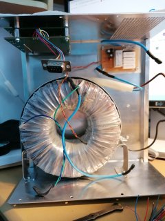
The initial design (for learning) was to use a 1Kw transformer and rectifier to get 120Vdc (at first), as a supply, then make a strong Buck converter to be able to variate the output voltage for Constant Voltage and Constant Current modes. So i started with a big transformer from microwave oven, witch i rewinded to output 88Vac at first, the difficult part was finding out how much voltage over the max 22s 92,4V was needed to achieve charging 12A, at first 120Vdc from supply was not enough, then i increased it to 130Vdc witch could drive 12A in the batt at full charge. Then the buck design, inductor size for 12A, mosfets(IRFP260) and diodes (MUR860) 2 in parallel, highside gate drive (IR2110), hall current sensor(ACS714-30A).
Next part was figuring a way to measure all 22 cells individually, with minimal error possible/acceptable. So i started looking at some balance chargers how do they do it, and i found that a cost effective and also accurate enough is to use multiplexers (HC4067) and good op amp(OPA4196) to measure differentially across 2 cells at a time, now one issue is the cell voltages need to be scaled down (voltage divider, 0.1% tolerance res.), all with the same ratio, so that the input at the mux-es is no higher than its supply (9v), and then scaled back with the op amp gain. The next part was the mux setting and sampling time of the uC ADC, so the conversion for cell voltages was put between 2 other different conversions and the mux setting was done in previous of cell conversion in order to have time to set and settle, this works great and is also simple to calibrate since the only considerable variable is the cell voltage divider tolerance.
Next part is cell balancing circuit, basically is a resistive load (0612 3R 4pc. in parallel) switched with a transistor between each 2 cells, and that array activated with shift registers (HC595).
Some details on de SW side, charger works in Constant Current mode as long as each cell is below 4,2V , pack voltage is under the selected pack xxSeries, and after those thresholds are reached it switches in to Constant Voltage mode, the balance works by comparing each cell voltage to the average voltage of all the cells and all cells that are higher then average get balanced continuously from the moment the pack is connected to the charger to the point the charge is stopped.
So far it works great on 10S 7,5Ah , 16S6P 12Ah, 16S7P 17Ah and 22s12p 60Ah Lithium batteries, with the mention that the higher the capacity the longer the balance time, because of 1A balance current. And so far the maximum charging power is 1,1Kw maximum.
This is a brief description of the charger, i'l explain each module in greater detail with schematic in the next posts, and the further development of this charger to achieve 3Kw.
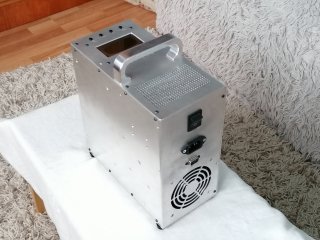
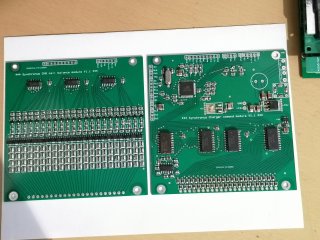
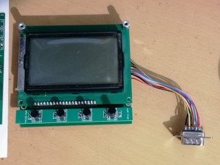
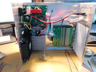
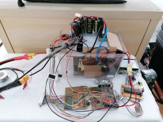
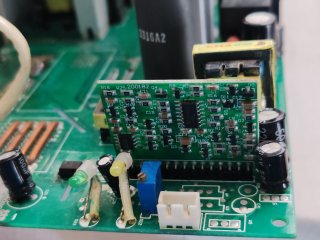
Here as some photos of the boards and the charger box.
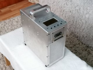
IMG_20230127_093753.jpgIMG_20230127_093806.jpgIMG_20221120_194754.jpg
 
A few more photos for now, the last one is from the development period, lots of wires and verry sketchy .
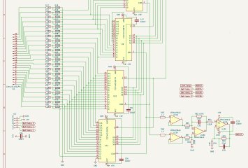
A part of the schematic with the cell selection and readout part.
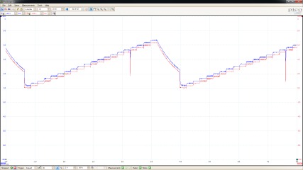
And an Osci shot when testing the cell readout on 20S batt, those are the outputs of the mux-es before the op amps

IMG_20221120_194808.jpgIMG_20221226_110816.jpgIMG_20221226_110832.jpgIMG_20201005_124754.jpgSch_bms_1.jpg
BMS  20s volt release 2.png
 
Last edited:
This is pretty cool, I'm curious what the efficiency is though with that big transformer and 1A resistive balancing. Have you thought about doing active 1A balancing instead of passive?
 
This is pretty cool, I'm curious what the efficiency is though with that big transformer and 1A resistive balancing. Have you thought about doing active 1A balancing instead of passive?
Well, the efficiency is not that great, and the power factor too. The upgrade is intended to exchange to SMPS, i have parts ( big ferrite transformer winded with thick copper foil :mrgreen:) from a damaged MIG/MAG welder, although that is a verry complex topic and will take some time to make work well (3Kw and mains is no joke :geek:), this is a starting point, High power adjustable switching power supply (SMPS) 3-60V 40A , DiodeGoneWild , that guy rocks with SMPS.
And yes active balancing to transfer charge between cells, but at this point i have no idea how to implement it, i will have to research on it, if any of you have any ideas please share.
 
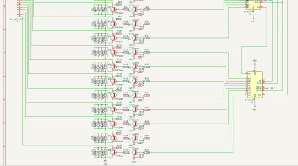
Here is part of schematic of the balance circuit, with the array of balancing resistors, their switches and the shift registers activators.
Now one big problem that i touched on another topic, is the cell sense/balance cables, particularly long ones like for a big 22s pack.
So these long-ish cables are the main limiting factor for cell balance current and also some readout error sometimes under load.
Now the trick for reading the cell voltages (in SW), is to do it while all balancing resistors are NOT active, in order to have true values, so the balancing circuit has a duty cycle of about 90% in order to have an "off window" to read the cells. A
And now we come to the Upgrade part where all those long cables cell sense can be minimized, and migrate the BMS out from the charger and put it on the battery side and still be disconnectable, me NOT like permanent hooked BMS on batt. And if that BMS is connected on the batt side it can communicate via RS232 with the charger and/or the controller, and this will mean the sense wires are way shorter and there resistance be small enough and compensated while doing cell balance and voltage measurement, plus the IR measurement is possible now, witch is a cool feature to have, but with long wire it is not possible due to cell sense wire residence error introduced. Side note to backup my point, i did some testing on an RC charger and "messed" with the length/thickness of cell sense wires, and that messed the cell IR measurement, the voltage was not affected because they read it smart, while balance is in inactive sate (off part of duty cycle).
Now the topic of active cell balancing, transferring charge from cell to cell, so in order to connect any cell to any cell in a 22s pack, the is needed some matrix multiplexer that can do that and also handle 1A current or more, or some way to connect each individual cell to a internal isolated supply to add more current to it and charge it faster , additive balancing as opposed to depletive balancing, this topic has many open points at this time.
1763124947619.png
 
Here is part of schematic of the balance circuit, with the array of balancing resistors, their switches and the shift registers activators.
Now one big problem that i touched on another topic, is the cell sense/balance cables, particularly long ones like for a big 22s pack.
So these long-ish cables are the main limiting factor for cell balance current and also some readout error sometimes under load.
Now the trick for reading the cell voltages (in SW), is to do it while all balancing resistors are NOT active, in order to have true values, so the balancing circuit has a duty cycle of about 90% in order to have an "off window" to read the cells. A
And now we come to the Upgrade part where all those long cables cell sense can be minimized, and migrate the BMS out from the charger and put it on the battery side and still be disconnectable, me NOT like permanent hooked BMS on batt. And if that BMS is connected on the batt side it can communicate via RS232 with the charger and/or the controller, and this will mean the sense wires are way shorter and there resistance be small enough and compensated while doing cell balance and voltage measurement, plus the IR measurement is possible now, witch is a cool feature to have, but with long wire it is not possible due to cell sense wire residence error introduced. Side note to backup my point, i did some testing on an RC charger and "messed" with the length/thickness of cell sense wires, and that messed the cell IR measurement, the voltage was not affected because they read it smart, while balance is in inactive sate (off part of duty cycle).
Now the topic of active cell balancing, transferring charge from cell to cell, so in order to connect any cell to any cell in a 22s pack, the is needed some matrix multiplexer that can do that and also handle 1A current or more, or some way to connect each individual cell to a internal isolated supply to add more current to it and charge it faster , additive balancing as opposed to depletive balancing, this topic has many open points at this time.
View attachment 380505
I'm no electrical engineer, but my intuition for active balancing would be several buck converters, and as you say, some form of multiplexer or switching to allow connecting to any of the cells. A simple algorithm to connect the highest voltage cell to the lowest voltage cell through the buck converter/charge circuit would probably do the trick. If you had for example 4 of them, then it could actively balance the 4 worst and 4 best groups continuously.

You could either add 7 more for 22s, do passive balancing for any remaining cells, have partial duty cycles, or find some more elegant way to do it probably. A 3a bucker converter suitable for charging a battery cell is just a few bucks as its own board at least. If it is only a buck converter than it automatically could only ever bring the cell groups to parity.

If allowing any cell to discharge to any other cell and vice versa requires too much switching logic, allowing each circuit to say connect to say 6 groups, with 8 circuits and careful overlap of them would have fully coverage if several extra balancing steps depending on which groups need to be balanced.
 
And yes active balancing to transfer charge between cells, but at this point i have no idea how to implement it, i will have to research on it, if any of you have any ideas please share.
Check out the datasheets, application notes, reference design, and evaluation boards that Texas Instruments and Analog Devices have for their active balancing chips. Even if you don’t use those chips there‘s a ton of info in those documents. Here’s one: https://www.ti.com/lit/ug/tidubz7/tidubz7.pdf
 
Thanks guys for your inputs, i'l investigate more on this topic as the time goes. At first glance, i got some ideas now, one way is to have, 11 isolated DCDC 5V supply's that can be connected by a switch matrix to odd or even cells at a time (which ever need balance), now 11 isolated 5v outputs can be achieved by having 11 secondary's on a isolated smps/buck transformer, it would have to be a 60W capable supply, to support 1A for all 11 outputs at once, which is not that hard to achieve by modifying an existing smps supply, rewinding the transformer and a custom board added with the rectifiers and filtering for all 11 outputs. The switch matrix mosfets would require isolated gate driving, optocouplers can be an option for that. At least now i have food for thought :mrgreen:
 
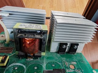
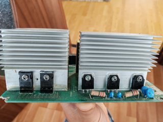
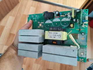
Started looking at the damaged welder board for salvaging the ferrite transformer, and did some reverse engineering, and figured its board topology, it is a 2 switch forward converter, it uses 4 IGBT-s (2 and 2 in parallel) IKW30N60H3 from infineon, and 4 (2 ans 2 in parallel) 60N30 double diode i think from fairchild, it is verry beefy, was a 5 kw welder, this is great, it's same topology i'l use for my charger supply to achieve 3kw ( or more :mrgreen: ), and i can use it's power switching devices with heatsinks and all the accessories that are around, the only concern that i have, is the transformer might not have enough voltage(higher than 100V) that i need, but this is verry dependent of supply output impedance and batt IR to determine the current magnitude, so this will have to be figured out in testing because i have no idea how to calculate it, i mean two "supplies" in parallel one sources(smps) one sinks(batt), so yeah... I'l draw its schematic in the next days and come back.
EDIT: not to be confused, that is a cheap ass welder, nothing fancy in it, and calling it beefy compared to what are my requirements for current.
here are some photos of the board and its bits.
1000047382.jpg1000047383.jpg1000047384.jpg
 
Last edited:
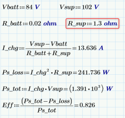
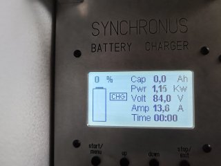
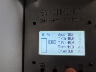
I'm back with some math/science, i managed thru testing and measurement to figure out a formula to calculate the supply's voltage to achieve a certain charge current. So i set the charger for 14A, and measured then, the batt was at 84v the supply voltage was at 102V under load (13.6A). As i said before the charging current is verry dependent of the supply's voltage and internal resistance/impedance, those are the main involved factors.
The formula is as follows:
1763623810431.png1763624608819.png
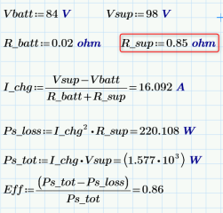
As you can see the dissipation is quite high in the supply, hence the "not so great" efficiency, 82%. The charger can do 16A max because 90% duty, and the dissipation is so high that it overheats due to loses, and at that current in about 30 seconds the 8A slow fuse on the mains blows up due to ripple and over load, witch indicates over 1,8Kw draw from mains, and that is why i limited at 12A continuous use and 14A max for 30 minutes.
This also shows the supply impedance/internal resistance affecting the current magnitude, and that 0,85ohm at 16A with 90% duty reflects the transformer secondary internal resistance (the greatest resistance in the current loop), which is about right.
1000047656.jpg1000047658.jpg
 
back with some updates, i begun to investigate what is broken on inverter welder board and then salvage the good parts, but then, i found that only the IGBT's, IKW30N60H3 all 4 ware shorted, in the primary side. So i decided to replace them, i had IKW50N60T "at hand", then checked everything else, all was fine, added cap's and a bridge, then powered it and see if it works, well, it outputs 65V no load, seems to be working. Then did some measurements and investigation, it switches at 66KHz, its control circuit is TL2845B.
Now, i'll start my development with that board, since it works, and i have to figure a way to control with a uC its control circuit (TL), it is better to have an ASIC controlling the supply and having all protections handled by it, and then have a uC just requesting needed voltage and current. Then i have to up the output voltage to 110-120V, one way to do it, is to increase the switching frequency to 100-120KHz, or the other way, is to add more turns in the secondary, witch is not that easy to do. And one important thing, is to KEEP the isolation from mains. So yeah, i'l start working on it.
 
i'm back with some math, again, i have done some calculations for the SMPS transformer, and it seems that obtaining a higher secondary voltage is not that simple with regard to increasing the switching frequency, because it affects the flux density in the core and it is still needed more turns in the secondary after all. It can be seen clearly in the calculation, so only option to up the voltage is adding more turns to secondary.
edit: or increase sw freq and reduce primary turns, but not desirable
1764168902703.png
 
Last edited:
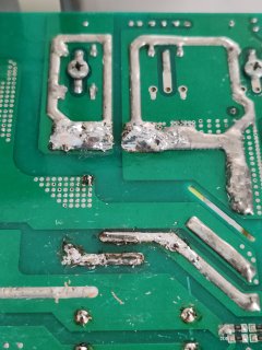
A bit of an update, i disordered the SMPS transformer from the board, i expected it to be extremely hard to take it off the board, the solder joints on the secondary ware very very beefy, but the 400W "soldering IRON" made this job piece of cake. This transformer is very "strong" winded with many copper foils in parallel, on the secondary the thickness is about 1mm and 10mm wide. Now i have to dismantle it and modify the windings, the tough part is that the secondary winding is between 2 primary windings , one inner one outer. One option is to split the parallel windings of the secondary in 2, and that allows double the turns and have half the thickness, witch is fine since i do NOT need 100-200A on the output, so half or 1/3 of that will be more than enough.
Here are some photos:
1000048299.jpg1000048298.jpg1000048295.jpg1000048320.jpg
 
A post about that iron would be interesting... ;)
Shure, here it goes :
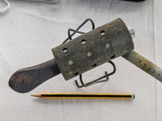
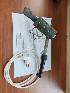
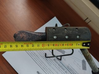
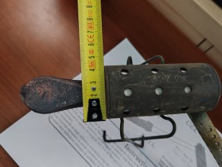
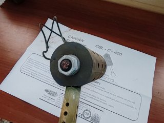
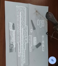
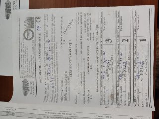
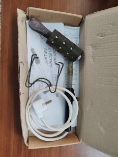
This soldering Iron is one of the few good things well built in the comunist era in our country, and the factory "survived" after that era ended, and they still produced it (a few years ago), you can see all the paperwork that comes in the packege, reflects it's "old" way of dooing things, still cool though. It's ergonomics are not that great, but it gets the job done and does not burn your hands at the handle, i was able to solder with it, huge 1mm thick busbars over the PCB in the past, being so big has a lot of thermal inertia and does not loose heat when soldering big stuff. Here are sone photos. 1000048368.jpg1000048369.jpg1000048370.jpg1000048373.jpg1000048367.jpg1000048374.jpg1000048377.jpg1000048376.jpg
 
Shure, here it goes :
This soldering Iron is one of the few good things well built in the comunist era in our country, and the factory "survived" after that era ended, and they still produced it (a few years ago), you can see all the paperwork that comes in the packege, reflects it's "old" way of dooing things, still cool though. It's ergonomics are not that great, but it gets the job done and does not burn your hands at the handle, i was able to solder with it, huge 1mm thick busbars over the PCB in the past, being so big has a lot of thermal inertia and does not loose heat when soldering big stuff. Here are sone photos.

Thank you for posting all that--I've never run across anything remotely like it (in many years of yard-sale / thrift store / industrial recycler / etc perusing).

Seems to be lots better than having to use a blowtorch to do this kind of work (I have a little mini propane torch I have had to use on occasion when my pinky-sized-tip 80w weller won't do it, or the 50w "spoon tip" thing meant for plastic smoothing doesn't either....)
 
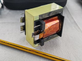
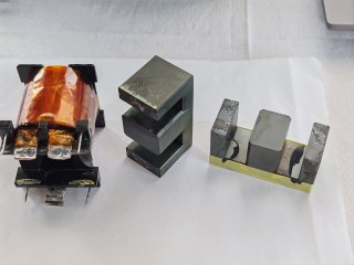
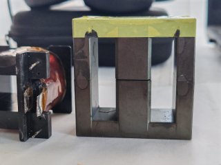
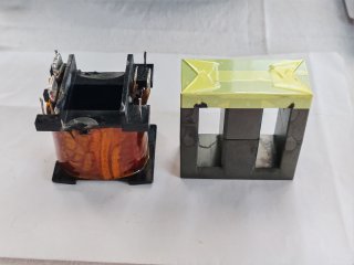
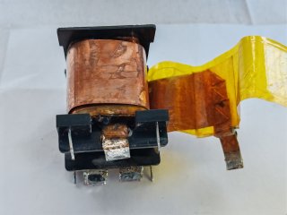
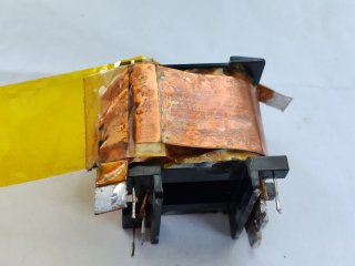
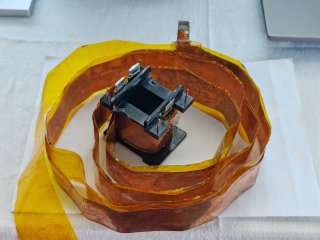
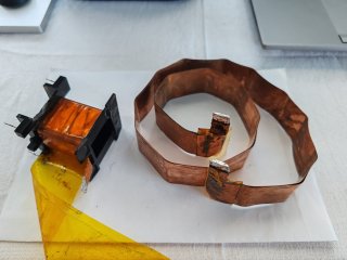
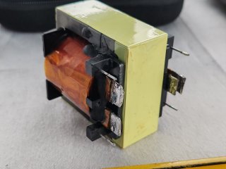
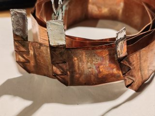
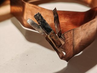
Back with updates, had great success dismantling the smps transformer, watched some "how to" on YT, then proceeded accordingly :mrgreen: . So i started by putting the transformer in a pot with water, and boiled it for 15 minutes in order to soften the resins, after that i tried to take it out, and while doing so, the E ferrite cores got detached, and pulled the thing in pieces out of the pot, good thing effortless disassembly. The E cores have 24.35mm by 16.86mm the center piece/tooth, 4.1sqcm area, and 40.72mm height, and it has air gap in the center piece/tooth. Then started to unwind the outer primary winding, came off nice and clean, it has 9 turns of single copper foil 0.09mm thick and 28mm wide. After that, started to unwind the secondary winding, also came off nice and clean, it has 5 turns of 3 copper foils in parallel, 0.09mm thick and 28mm wide, each, beefy stuff. A cool technique to make the end terminals of the winding is seen here, they split in 3 the foil width and bent it 90degres outward, then soldered all 3 ends in parallel to have same area but smaller width for the terminal, cool stuff (in the 4-th photo). Now i'l think of a way, to split the secondary foils in order to get 10 turns in the secondary.
EDIT: the secondary foil thickness is 0.09mm instead of 0.18mm that i initially stated wrong.
Here are some photos:
1000048829.jpg1000048831.jpg1000048832.jpg1000048833.jpg1000048834.jpg1000048835.jpg
1000048836.jpg1000048838.jpg
 
Last edited:
Back with update, i rewinded the pulse transformer: So, one foil has 2,52sqmm(0.09x28mm), initially the 3 parallel foils had 7.56sqmm total, i decided to split the 3 parallel foils in 2, and that means one foil was cut in half, now the total area is 3.78sqmm, then soldered the obtained 1,5 foils end to end, and then winded 10 turns on the secondary, i did had to redo the winding end terminations in order to fit them in the designated termination slot of the bobbin. Cleaned and prepped the holes and slots in the PCB where the transformer is mounted, installed mains bridge rectifier and the caps in there correct form and place (before for testing ware just wired sketchy). Before i solder back the transformer in its place, i'l connect it with wires for testing, to check it's correct function, and if all ok, i'l put it back. I need to add an output inductor since now it does not have one (see the 4 parallel thick wires on the PCB) Now, before power up, i need to check the circuit components in the feed back loop, since the output voltage will be double , expected 120V and nothing blows up, and find a way to control the SMPS converter ASIC externally to vary the output voltage, so i need to reverse engineer its control circuit first.
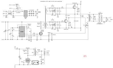
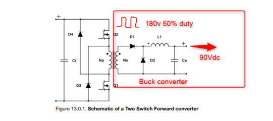
Here is a typical schematic of 2 switch forward converter for inverter welder (found on net, author is written on it), my board is 90% made like that, the main difference is in the control circuit, has a bit more complexity, but the control ASIC is the same family/type.
Here are some photos:
1764924274111.png1000049076.jpg1000049078.jpg
1000049101-jpg.381682
1000049105.jpg1000049106.jpg
 

Attachments

  • 1000049101.jpg
    1000049101.jpg
    2.6 MB · Views: 56
I'm back with progress, after a bit of reverse engineering of the smps control board, i figured that output voltage is not considered in the control loop circuitry, it only takes in to account the primary current and a setting of minimum and maximum current from a pot. So i connected the transformer with wires for the moment (testing), no output inductor and capacitors yet, and powered the thing.
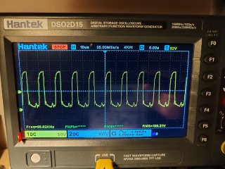
It outputs with no load 130V at minimum current setting (low duty cycle), and goes above 250V at max current setting (max duty cycle), and of course the output being unfiltered yet the ripple is huge. With a 200W light bulb as a load, it outputs 89v at max current setting, same here massive ripple, so the voltages are a bit "off" from what they will be after output filtering is added. Now to control/regulate the output voltage, the smps control ASIC has a voltage feedback pin that can be used tor that, but in welder application it is not used, so that function will be added/implemented. The scope shot is ASIC PWM output, but with floating ground, since the primary side is mains connected, i'can not connect the ground lead of the probe to the minus of the rectified mains, differential probe is needed here.
Here are some photos of the moment:
1000049609.jpg1000049624.jpg1000049611.jpg
 
yet an other update folks,
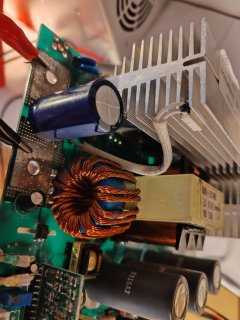
I mounted the output inductor ~12uH, it has 9 turns of 24strands of 0,5mm copper wire, wound on 2 pc. 30mm OD iron power cores, also added an 470uF output cap, and mounted the transformer back in its place.
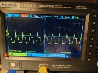
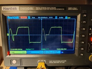
Did some measurements with a ~300w load on it, the output with inductor and without cap has 106,3V (first pic. scope)
Second scope pic is the transformer secondary out (before rectifier)
The output with the cap added, has 97V dc (with 300w load),
Next i'l try to load it up to about 2-3kw depending on what resistive load i can find, and see what voltage it has on the output
EDIT: the power levels corrected
Here are the photos:
1000050103.jpg1000050104.jpg1000050106.jpg
 
Last edited:
back with some tests, progress and conclusions/not :mrgreen: :
1. I striped off all welder specific functions, only the overcurrent limitation is present,
2. I gained access to the VFB pin of the smps ASIC, and configured it to run in open loop, with a potentiometer varying the output, voltage from about 4V up to max (75-95V), and this "max" is the next point,
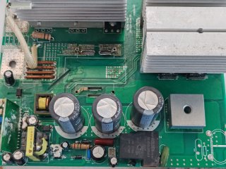
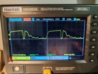
3. So, with inductor and capacitor on the output, i could load it (did not have a "lower" resistance load) 5.4A at 75V "max" smooth dc, if i removed the output inductor and the capacitor, with the same load applied, it drown 7.1A at 95V "max" but with big ripple, conclusion the inductor reduces the output voltage but you get smooth Vdc on output. The DMM on no inductor and cap test, showed 95V and oscilloscope showed 118Vrms. Now the big question is, in order to charge a battery, do i need smooth dc, or is just fine with ripple, one thing to consider is that the battery will act like a big capacitor on the output of smps. Another thing to note is that on the actual charger with transformer due to high output currents, the DC-Link caps on the supply, do not keep the voltage smooth, and it also has considerable ripple at double the mains freq (100Hz), and all this, translates in current ripple, and the main problem was, the current sensing need serious SW and HW filters in order to have a stable and accurate current reading in order to calculate realistically the amp hours capacity charged in the battery.
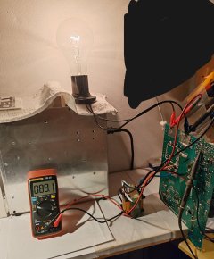
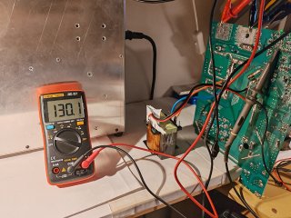
4. Next step, i need to connect on the smps output a hall current sensor to be able to read 30A, and i'l try to hook up the 22s plane battery, and see how much current can smps push in it.
here is a scope shot of the loaded without inductor and cap test, that showed 118Vrms on output
1000050214.jpg
 
Back with a bit of science, last weeks of last year during testing, i got to the edge of my knowledge, and started to study the "appropriate literature" in the SMPS field, to find answers to some question that i had.
So, I found out that the two switch forward converter, the circuit after the secondary can be treated in theory like a buck converter, so at max duty 50% i get on the secondary ~180V Pk-Pk on the output, witch yields ~118Vrms, and after the diodes inductor and capacitor circuitry which is a buck converter in theory of work, i get about 90V dc depending on load, and that is the reason of voltage reduction on output, basically a buck converter that operates at 50%duty reducing the ~180v to ~90v.
Now the next steps, more study and calculation must be done, before proceeding forward.
"literature": https://www.ti.com/lit/eb/slyu036a/...chTerm%3Dpower+topologies+handbook%26nr%3D320
1768386927489.png
 
And yes active balancing to transfer charge between cells, but at this point i have no idea how to implement it, i will have to research on it, if any of you have any ideas please share.
You might consider dropping the matrix strategy and go another easier route: only compare and balance between adjacent cells (with inductive method). It would reduce complexity from order n^2 to order n.

(The idea is from simple '1.2A Active Balancer' boards like this https://de.aliexpress.com/item/1005006065244684.html)
 
Back
Top