Hi all,
I thought I'd share - and hope to get some feedback on a pack I'm building.
Nothing against welding nickel tabs on 18650 cells - they work reliably for me as well.
But, I wanted to experiment with connecting cells - no welding or soldering.
Here's the design.
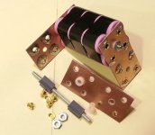
See attached photo.
1. Groups of (4) 18650 cells are connected in parallel using a double sided PCB. (I'm using Samsung 35Es).
Each board connects two 4 cell groups of the
in series. Plus on one group to Minus on the other.
(9) boards are required for a 10S pack. I'm using plain FR4 material with
1oz copper on each side. Boards are cut on a fine tooth carbide chop saw, and
'drilled' out on my small CNC mill.
2, Each of the 8 cell contact holes in the board are filled with a brass eyelet, crimped, then soldered
to make good electrical and mechanical connection from one side of the board to the other. (no plated
through boards required.)
The head side of the eyelets provides a raised bump to make contact with the center of each cell on either the
positive or negatives ends. I've tinned the head of the eyelets to prevent oxidation.
3. Each group of 4 cells is held in a controlled square pattern - matching the PCB eyelet pattern, by inserting
two 3D printed spacers in the center gap. See the grey pieces in the photo. This locks together the 2X2 array when tightly
taped.
4. The PCB, cell, spacer, assembly is clamped together with 8-32 all thread rods and nuts. TWO NYLON SHOULDER WASHERS
are used, to insulated the 8-32 rod from the PCB connections. Deflection of the PCB and tension in the approx. 3" rod provide
the 'spring' to assure good 4 cell conctact (so far so good).
5. ADVANTAGES: Cell groups or individual cells easily replaced. Connections from each 4 cell group to BMS is a simple solder
connection. And pack power connections are equally simple soldered cables (12ga stranded). All materials are readily available and low cost. (you could get a mail order house to make the PCB but this method doesn't need etching, solder mask, silkscreen, or plated through holes. )
6. DISADVANTAGES: temperature, corrosion, stability long term TBD.....
Please weigh in with any thoughts - I might try copper rivets with the next one instead of brass eyelets.
I thought I'd share - and hope to get some feedback on a pack I'm building.
Nothing against welding nickel tabs on 18650 cells - they work reliably for me as well.
But, I wanted to experiment with connecting cells - no welding or soldering.
Here's the design.
See attached photo.
1. Groups of (4) 18650 cells are connected in parallel using a double sided PCB. (I'm using Samsung 35Es).
Each board connects two 4 cell groups of the
in series. Plus on one group to Minus on the other.
(9) boards are required for a 10S pack. I'm using plain FR4 material with
1oz copper on each side. Boards are cut on a fine tooth carbide chop saw, and
'drilled' out on my small CNC mill.
2, Each of the 8 cell contact holes in the board are filled with a brass eyelet, crimped, then soldered
to make good electrical and mechanical connection from one side of the board to the other. (no plated
through boards required.)
The head side of the eyelets provides a raised bump to make contact with the center of each cell on either the
positive or negatives ends. I've tinned the head of the eyelets to prevent oxidation.
3. Each group of 4 cells is held in a controlled square pattern - matching the PCB eyelet pattern, by inserting
two 3D printed spacers in the center gap. See the grey pieces in the photo. This locks together the 2X2 array when tightly
taped.
4. The PCB, cell, spacer, assembly is clamped together with 8-32 all thread rods and nuts. TWO NYLON SHOULDER WASHERS
are used, to insulated the 8-32 rod from the PCB connections. Deflection of the PCB and tension in the approx. 3" rod provide
the 'spring' to assure good 4 cell conctact (so far so good).
5. ADVANTAGES: Cell groups or individual cells easily replaced. Connections from each 4 cell group to BMS is a simple solder
connection. And pack power connections are equally simple soldered cables (12ga stranded). All materials are readily available and low cost. (you could get a mail order house to make the PCB but this method doesn't need etching, solder mask, silkscreen, or plated through holes. )
6. DISADVANTAGES: temperature, corrosion, stability long term TBD.....
Please weigh in with any thoughts - I might try copper rivets with the next one instead of brass eyelets.