lazarus2405
10 kW
So I'm in the process of modifying my Milwaukee packs for ebike use. I'm simply soldering 10AWG to the battery tabs to bypass the BMS for discharging, leaving it intact for easy charging using the stock charger and BMS. Of my six packs, one isn't working. If I can't use the BMS to charge, then I have to find some other solution, which from what I can figure it won't be nearly as simple. So please, help me troubleshoot the problem.
So, my symptoms: the pack won't charge.
The charger recognizes the pack, and reads it as being full. (It has a separate readout for a "faulty" pack for various reasons.) It's reading around 27.4V (nominal is 28V, hot off the charger is ~29.1) at the tabs (before the BMS); its built in "Power Meter" reads ~30%.
All balancing leads are intact; I'm sure of that. All cells are level (~3.92V), with no faulty or low cells.
The voltage across the discharging leads varies very quickly. It starts around 30mv and climbs to ~300mv, then drops again to 30. These are the discharge leads made to connect to the tool, so it should be in the 28V neighborhood.
The BMS sits between the negative discharge lead and the negative battery tab. There is no path between the two (resistance beyond my DVM's range).The connection between the BMS and neg battery tab is secure.
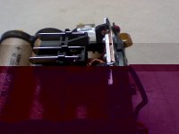
So, the negative discharge lead is the positive lead for charging. This connects to an aluminum plate that acts as a heatsink, which connects to the copper sticking out of the two IRF4104 MOSFETS in parallel (which appear to be completely intact). I cannot tell what else this aluminum bit connects to electrically, but I think that it acts as the third connector of the MOSFET. Right, wrong? The two MOSFETs connect to the BMS's PCB with the two outside legs, not a middle.
So, what's the DVM say? Well, the voltage between the positive battery tab and any of the four MOSFET legs is pack voltage. Voltage between the two legs of each respective MOSFET is 1.6mV, and resistance is 1.2kOhm. Resistance between any MOSFET leg and any part connected to its heatsink is something like 7.4MOhm.
The BMS PCB is covered by a spray-on insulating gel sort of thing, so as far as I know it's undamaged. It also means that I can't trace the circuits, but if you tell me what to look for I can dig around. I'll post some pictures below in a bit. If you have any suggestions, or if you need any more information whatsoever, just speak up. Thanks


