signalab BMS 24 channel defect??

nono. you should go to ping's website where he has the diagrams. there should not be any lead from the top B+ of the battery to the BMS. none.

the P- connects to the controller negative.

the B- connects to the bottom of the battery, B-

the C- connects to the negative lead of the charger.

remove everything else.

if you still have the sense wires connected to the battery disconnect the sense wire plug from the BMS until you can repair the BMS. if the cells continue to read in the 4.2V range while they are attached to the BMS through the sense wires then the BMS is dead now. it means the p channel mosfets used as the balancing transistors are blown open circuit. usually they are shorted so that is unusual too.

but first thing is to remove any high voltage from the BMS. it should never be there. the BMS is essentially a fuse in the negative battery lead. if you have full pack voltage on it when it shorts out then it can cause big problems. but it has to be rewired properly, and if it is still functional then we can show you how to hack it to 22S but i suspect there is some reason we do not yet know as to why there is no charging mosfet on there.
 
dnmun said:
nono. you should go to ping's website where he has the diagrams. there should not be any lead from the top B+ of the battery to the BMS. none.

the P- connects to the controller negative.

the B- connects to the bottom of the battery, B-

the C- connects to the negative lead of the charger.

remove everything else.

if you still have the sense wires connected to the battery disconnect the sense wire plug from the BMS until you can repair the BMS. if the cells continue to read in the 4.2V range while they are attached to the BMS through the sense wires then the BMS is dead now. it means the p channel mosfets used as the balancing transistors are blown open circuit. usually they are shorted so that is unusual too.

but first thing is to remove any high voltage from the BMS. it should never be there. the BMS is essentially a fuse in the negative battery lead. if you have full pack voltage on it when it shorts out then it can cause big problems. but it has to be rewired properly, and if it is still functional then we can show you how to hack it to 22S but i suspect there is some reason we do not yet know as to why there is no charging mosfet on there.

Ok for the love of....

Anyway i rewired as per your specs... when i connected the BMS sensing wires all the same six leds came on. I checked the voltages and the highest was now 3.8 ... 5 mins later, and now 5 lights are on and high voltages are 3.555, 3.691, 3.600, 3.597,3.662,3.634......

Ive included a diagram of the re-wired BMS

i wait..a couple of mins later they are beginning to flash, some blinking, 2 have gone off...eventually they all go off.. i remeasure the voltages of the affected strings.....all voltages are 3.29 volts and the highest voltages previously measured are now 3.540, 3.599, 3.598, 3.593,3.5 and 3.51.

So, i hooked up the charger WHILE watching voltage from my multimeter and right away 4 then 5 then 6 lights come on and voltages going from 3.5 to 3.8 to over 4 volts...i quickly disconnect and once again the lights begin flickering on and off and eventually off...voltages come down to normal

OK so im assuming that 1 ) the BMS is working BUT because it has no Charging Mosfet indicated in diagram ...that it cannot control the max voltage?

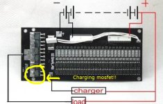
The photo of the BMS when i went to purchase indeed looks to have the Charging mosfet or am i wrong?chrgin mosfet.jpg


missing chg.jpg
wiring endless.jpg


John
 
yes, the charging mosfet is how the current goes from the charger to the battery. but without the 2 cells it should still not charge. the LVC should turn off the output mosfets that are still there.

if the leds turned off when it dropped below 3.6V on that channel then the balancing transistors are still functional.

edit, i just went and looked at the 20S signalab i have here and there are two charging mosfets in parallel so that is why yours looks like that. it still has the one mosfet in the second spot. i thought that was one of the output mosfets.

so the charging mosfet there may be shorted. does it get hot when you charge? do the output mosfets get hot?

can you measure the voltage on the gate legs of the charging mosfet and the other mosfets?

put the red probe on the left leg and the black probe on the B- spot. should be about 5.7V on the charging mosfet and 13.7 on the output mosfets.
 
dnmun said:
yes, the charging mosfet is how the current goes from the charger to the battery. but without the 2 cells it should still not charge. the LVC should turn off the output mosfets that are still there.

if the leds turned off when it dropped below 3.6V on that channel then the balancing transistors are still functional.

edit, i just went and looked at the 20S signalab i have here and there are two charging mosfets in parallel so that is why yours looks like that. it still has the one mosfet in the second spot. i thought that was one of the output mosfets.

so the charging mosfet there may be shorted. does it get hot when you charge? do the output mosfets get hot?

can you measure the voltage on the gate legs of the charging mosfet and the other mosfets?

put the red probe on the left leg and the black probe on the B- spot. should be about 5.7V on the charging mosfet and 13.7 on the output mosfets.

Ok...if by gate legs you mean the three protrubences sticking out of the 5 charging mosfets ( i illustrated what i did on a diagram) then when i plugged it in to charge there was no reading at all.

I tested all 5 and no reading on any. The little ones (output mosfets?) of which there is 24 on top and 24 on the bottom correspond the individual cell voltages and the lights that were flashing all had voltages over 3.5

Yes initially, where the P- is it got very hot, but i cant put it on the charger for any more than a few seconds as the voltages go over 4 volts

John
 
dnmun said:
all the mosfets are shorted. measure the left leg, you put in an arrow pointing to the right leg. really doesn't matter. just start over with another BMS.

Or i guess i could replace the 5 mosfets....would be cheaper

Thanks for all your knowledgeable help!!!

John
 
you just don't seem to be familiar with the parts so not sure it is something you would do.

if you remove the BMS from the wiring, you can test the mosfets with the diode tester on your voltmeter.

the gate is always insulated from the source and rain so it will always be open circuit, but the body diode of an n channel enhancement mode mosfet will conduct current from the source to the drain and you can measure the body diode with the diode tester function on your meter. should be 400-500mV.

then if you reverse the probes and put the red probe on the drain, or tab, and the black probe on the source leg, then it should be open circuit on the diode tester. it will have a 1 on the left side of the display, no numbers displayed.

if it conducts when you have the red probe on the drain and the black probe on the source then the mosfet is shorted.
 
dnmun said:
you just don't seem to be familiar with the parts so not sure it is something you would do.

if you remove the BMS from the wiring, you can test the mosfets with the diode tester on your voltmeter.

the gate is always insulated from the source and rain so it will always be open circuit, but the body diode of an n channel enhancement mode mosfet will conduct current from the source to the drain and you can measure the body diode with the diode tester function on your meter. should be 400-500mV.

then if you reverse the probes and put the red probe on the drain, or tab, and the black probe on the source leg, then it should be open circuit on the diode tester. it will have a 1 on the left side of the display, no numbers displayed.

if it conducts when you have the red probe on the drain and the black probe on the source then the mosfet is shorted.

I really appreciate the feedback however, when giving instructions to someone, one must not assume the reader knows as much as your assuming i know otherwise i could probably diagnose this myself. I dont know what a GATE is, i know what a DIODE is but not a BODY DIODE...i dont know what a SOURCE LEG is ....if you could explain in laymans terms i would appreciate it


Thanks

John
 
i don't know what ping uses, but for 100V you can google the data sheet for the IRFB4110 and they have pictures of the legs too, but this is what a mosfet its.

http://en.wikipedia.org/wiki/MOSFET
 
dnmun said:
you just don't seem to be familiar with the parts so not sure it is something you would do.

if you remove the BMS from the wiring, you can test the mosfets with the diode tester on your voltmeter.

the gate is always insulated from the source and rain so it will always be open circuit, but the body diode of an n channel enhancement mode mosfet will conduct current from the source to the drain and you can measure the body diode with the diode tester function on your meter. should be 400-500mV.

then if you reverse the probes and put the red probe on the drain, or tab, and the black probe on the source leg, then it should be open circuit on the diode tester. it will have a 1 on the left side of the display, no numbers displayed.

if it conducts when you have the red probe on the drain and the black probe on the source then the mosfet is shorted.


Ok so ive included a picture so i know im on the right channel with you...im assuming you meant DRAIN not RAIN...so

I put the red probe on my voltmeter in diode mode on the drain and the negative probe on the source i got 0.120 on the first 4, the 5th one read 0.000

When i put the red probe on the source and black on the drain i read 0.000 on all
so this means???

So for heck i checked continuity from the gate and the source and the first 4 show no continuity but the last one sure does..

mosfet.jpg


John
 
so the 5th one is the one on the left next to that empty spot? like i said, i found one of the 20S v2.5 signalabs i had for parts and it has 2 charging mosfets. so if that is the charging mosfet that would account for your failure to prevent overcharging. your charger voltage may be too high too.
 
dnmun said:
so the 5th one is the one on the left next to that empty spot? like i said, i found one of the 20S v2.5 signalabs i had for parts and it has 2 charging mosfets. so if that is the charging mosfet that would account for your failure to prevent overcharging. your charger voltage may be too high too.

Yes the fifth one is the one beside the empty slot. So your saying that this is the charging mosfet? and that it is shorted out?. so if this is the charging mosfet then the other 4 are the output mosfets?..they all look exactly the same....

The charger i bought is 87 volts...the BMS is designed to handle 87 volts.

John
 
Ok so im getting another one and this time know how to hook it up...so how do i mod it to use 22 channels instead of 24??


I really appreciate all the feedback on this issue, very much appreciated!!


John
 
on the v2.5 signalab you will wire each channel in order for 1 to 22. the bottom of #1 cell goes to the B- spot on the BMS, and the top of #1 is the black wire that goes in the first sense wire spot.

the top two channels will then need for you to bypass the top two opto transistors in the LVC chain. that is the series of optos on the inside. the outside has the opto chain that goes down to the charging mosfet.

if you look on the underside you will see how the outer opto chain has those two trace running side by side down the pcb all the way to the gate on the charging mosfet. that HVC opto chain is how the charging mosfet is turned off when one cell reaches HVC.

the inside chain is for the LVC, and since the top two channels are missing, the two opto transistors will not be turned on so the voltage signal that comes onto the top leg of the top opto (the collector of the transistor) does not get transferred down to the top of #22 where the first active opto transistor is present and is turned on by the cell in that channel.

so what you have to do is to solder a jumper wire from the top leg of the top opto down to the bottom leg of the opto transistor on the 23rd channel. that carries the voltage signal around the two missing channels.

then the BMS will function normally on the 22 channels present.

so now you understand about the body diode of the mosfet? to test the mosfets you put the meter into the diode function, then put the red probe on the middle leg(or the tab) and the black probe on the source leg, (the leg on the right side) and the meter should show the 1 on the scale over on the left side to indicate open circuit.

then you reverse the probes, put the red probe on the source leg and the black probe on the drain, or tab. the body diode should conduct in this direction. the gate leg on the left is insulated from both the source and drain so if you put the probes between the gate and drain or the source they should both read open circuit.

but that is just the output and charging mosfets. since you had skipped two channels in the middle of the source of the voltage for the circuit current when you skipped channels 3 and 4, there was only about 6.5-7V to drive the little black 14 pin comparator IC on the backside that drives the gates of the output mosfets so it may be damaged by low voltage too. but there is no way to know unless you properly rewire the BMS sense wires like i said and put the jumper on the top two optotransistors as detailed above.

then there is the little mosfets on each channel that turn on to divert current around the cell when it reaches the balancing voltage. it is not clear if they are still functional. if they are damaged they will drain the channel down to zero volts.

those little mosfets are just like the big one, source, drain and gate all present. except they are p-channel mosfets, the output mosfets are n-channel mosfets. so the body diode is reversed in those mosfets but you test them the same way.

if you look at the traces going from the sense wire plug down to the little p-channel mosfet, you will see it goes to the lower side leg. that is the source leg. the other leg on the upper side is the gate. the leg on the other side of the mosfet is the drain.

so to test them you would do the opposite of the n-channel mosfet. put the red probe on the source, black on the drain and it should be open circuit. put the red probe on the drain and the black probe on the source and the mosfet should conduct through the body diode and you will measure about 595mV forward bias for the body diode of the little mosfets.

so that is what it takes to determine if the BMS will still function. if they are dead, you are limited in your options. i have replaced the small mosfets and the gate driver, the little 5 pin IC on the underside connected through that via. it was very difficult. very very difficult.
 
Ok the new BMS will be here next week....im going to try and figure out your instructions from someone who is a lay person and not familiar with most of these terms.

"on the v2.5 signalab you will wire each channel in order for 1 to 22. the bottom of #1 cell goes to the B- spot on the BMS, and the top of #1 is the black wire that goes in the first sense wire spot."...ok i got this
"the top two channels will then need for you to bypass the top two opto transistors in the LVC chain. that is the series of optos on the inside. the outside has the opto chain that goes down to the charging mosfet."..... opto transistors??... LVC chain?....series of optos on the inside?? im assuming the 5 big things in the front are the charging mosfets correct?

"if you look on the underside you will see how the outer opto chain has those two trace running side by side down the pcb all the way to the gate on the charging mosfet. that HVC opto chain is how the charging mosfet is turned off when one cell reaches HVC."

outer opto chain? pcb?

"so what you have to do is to solder a jumper wire from the top leg of the top opto down to the bottom leg of the opto transistor on the 23rd channel. that carries the voltage signal around the two missing channel"

??

BABY STEPS

John
 
on the v2.5 signalab you will wire each channel in order for 1 to 22. the bottom of #1 cell goes to the B- spot on the BMS, and the top of #1 is the black wire that goes in the first sense wire spot.

the top two channels will then need for you to bypass the top two opto transistors in the LVC chain. that is the series of optos on the inside. the outside has the opto chain that goes down to the charging mosfet.

if you look on the underside you will see how the outer opto chain has those two trace running side by side down the pcb all the way to the gate on the charging mosfet. that HVC opto chain is how the charging mosfet is turned off when one cell reaches HVC.

the inside chain is for the LVC, and since the top two channels are missing, the two opto transistors will not be turned on so the voltage signal that comes onto the top leg of the top opto (the collector of the transistor) does not get transferred down to the top of #22 where the first active opto transistor is present and is turned on by the cell in that channel.

so what you have to do is to solder a jumper wire from the top leg of the top opto down to the bottom leg of the opto transistor on the 23rd channel. that carries the voltage signal around the two missing channels.

then the BMS will function normally on the 22 channels present.


Ok in anticipation of the new BMS, im going to present a diagram and point to what i think your talking about so i can "hack" this thing properly.
1st, i started with the 1st black sensing wire on the battery not the B- spot. Since the diagram shows the B- spot and the 1st neg wire on the same circuit im supposing it doesnt matter?. I then wired them in order and am left with 1 red sensing wire at the other end. If it does matter please explain why.

On the diagrams i will number different components, and you can tell me which is which...
board bms.jpg


what number on the diagram are the opto transistors ? ("bypass the top two opto transistors in the LVC chain")
where is the charging Mosfets? (K , L, and M i presume?)
board bms 2.jpg
board bms3.jpg

What is the pcb?

Finally since im left with one red sensor wire do the instructions to hack this board differ ?

Thanks

John
 
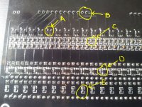
A is the comparator/gate driver for the balancing shunt transistor on the other side.
B is the soldered legs of the sense wire plug.
C is the current limiting resistor and cap for current supply to the comparator in A.
D is the HVC and LVC comparator/led driver for the optotransistor, and the 103 resistor next to it is the current limiting resistor that drives the led in the LVC optotransistor.
E is the current limiting resistor for the HVC optotransistor led.
K are the protection diodes on the current supply to the 14 pin IC
J is the 14 pin IC that controls the output transistors by supplying the gate voltage to control the output mosfets.
O is the balancing shunt transistor.
F,I are output mosfets.
M is the charging mosfet connected through the source leg to the C- spot.
N is one of the LVC opto transistors. the top two optos in this chain are the ones you have to bypass by soldering a jumper around them from the top or collector of the top opto down to the bottom or emitter of the 23rd opto. you can google the part number F817B to get the data sheet and it shows a picture of how the opto is built and which legs are which.

you can solder the jumper to the legs where they are soldered into the pocb on the underside or solder directly to the legs on top.

pcb is the abbreviation for printed circuit board.
 
dnmun said:
A is the comparator/gate driver for the balancing shunt transistor on the other side.
B is the soldered legs of the sense wire plug.
C is the current limiting resistor and cap for current supply to the comparator in A.
D is the HVC and LVC comparator/led driver for the optotransistor, and the 103 resistor next to it is the current limiting resistor that drives the led in the LVC optotransistor.
E is the current limiting resistor for the HVC optotransistor led.
K are the protection diodes on the current supply to the 14 pin IC
J is the 14 pin IC that controls the output transistors by supplying the gate voltage to control the output mosfets.
O is the balancing shunt transistor.
F,I are output mosfets.
M is the charging mosfet connected through the source leg to the C- spot.
N is one of the LVC opto transistors. the top two optos in this chain are the ones you have to bypass by soldering a jumper around them from the top or collector of the top opto down to the bottom or emitter of the 23rd opto. you can google the part number F817B to get the data sheet and it shows a picture of how the opto is built and which legs are which.

you can solder the jumper to the legs where they are soldered into the pocb on the underside or solder directly to the legs on top.

pcb is the abbreviation for printed circuit board.


Ok i got the new BMS in. The data sheet for the part number F817B is incomprehensible for the limited number of pages i found for it. Ive once again included a diagram of the new board and where i think you want me to solder a jumper around the top 2 opto transistors. However a couple of things first.
When wired to all of my cells im left with 1 positive wire as im using 3 different batteries and each of the three get connected together in series to one another as this was the only way to fit this configuration of batteries in the battery box The first 9 wires starting with the negative wire on the 1st battery ( the negative wire is hooked up to the first group of 16 cells), the next 6 go to the middle battery, continuing with the the last battery of 8 wires, leaving the last one (the positive unhooked). So do i still have to bypass the 2 opto transistors?. The other thing that happened is when the charging went over 4.3 volts i lost 16 batteries...all drained down to almost zero volts, and strangely coated with something, almost if the battery ruptured..i tried charging them but they would not take a charge. So i had some left over lifepo4 batteries that im replacing these with.

Ive number the opto transistors..please indicate what i have to solder to what....

A question; not doing this hack will result in what?

Thanks

John
 
where you have neg-, that is where the sense wire from the top of #1 goes. the bottom of #1 is B- so that is where it makes the connection for the bottom of #1.

the inside row of opto transistors is used for the LVC signal. since you will not have any cells on channels 23 and 24 then it will not be able to turn on the optotransitor to transfer the LVC signal down to the 14 pin IC that uses the LVC signal to control the output mosfets.

there is nothing hard about reading the data sheet. you will see there is a diode on the input side and a transistor on the output side. the light from the led turns on the transistor. the current goes through the transistor from collector to emitter, top to bottom.

since the led is not lit because there is no cell there to provide current to ignite it on that channel, the transistor is not turned on for 23 and 24 so it will not allow you to charge because the output mosfets have to turn on in order for the charging current to flow through them to the battery. the output mosfets are turned off when they do not get the current flowing down that chain of transistor in the opto transistors.

so take a tiny wire, it is easiest on the underside, and connect the top leg of the #24 opto, down to the bottom leg of the #23 opto. it can touch all four of the legs but it only has to be soldered to the top of 24 and the bottom of 23. you will confirm it from looking at the picture in the data sheet. so you will actually know what you are doing when you do it.

when it is soldered then you can solder The BMS to the battery at B-, solder the negative charger lead at C-, and then connect the sense wires from 1-22 sequentially and of course you now know to leave 23 and 24 empty.

http://www.mouser.com/ds/2/149/Fairchild%20Semiconductor_foffod617a-277596.pdf

you can see from the picture that the collector is leg #4 and the emitter is leg #3.
 
dnmun said:
where you have neg-, that is where the sense wire from the top of #1 goes. the bottom of #1 is B- so that is where it makes the connection for the bottom of #1.

the inside row of opto transistors is used for the LVC signal. since you will not have any cells on channels 23 and 24 then it will not be able to turn on the optotransitor to transfer the LVC signal down to the 14 pin IC that uses the LVC signal to control the output mosfets.

there is nothing hard about reading the data sheet. you will see there is a diode on the input side and a transistor on the output side. the light from the led turns on the transistor. the current goes through the transistor from collector to emitter, top to bottom.

since the led is not lit because there is no cell there to provide current to ignite it on that channel, the transistor is not turned on for 23 and 24 so it will not allow you to charge because the output mosfets have to turn on in order for the charging current to flow through them to the battery. the output mosfets are turned off when they do not get the current flowing down that chain of transistor in the opto transistors.

so take a tiny wire, it is easiest on the underside, and connect the top leg of the #24 opto, down to the bottom leg of the #23 opto. it can touch all four of the legs but it only has to be soldered to the top of 24 and the bottom of 23. you will confirm it from looking at the picture in the data sheet. so you will actually know what you are doing when you do it.

when it is soldered then you can solder The BMS to the battery at B-, solder the negative charger lead at C-, and then connect the sense wires from 1-22 sequentially and of course you now know to leave 23 and 24 empty.

http://www.mouser.com/ds/2/149/Fairchild%20Semiconductor_foffod617a-277596.pdf

you can see from the picture that the collector is leg #4 and the emitter is leg #3.

Ok heres a diagram as i understand your instructions....please verify if this is correct.
wiring hack.jpg

Thanks

John
 
i don't follow why you decided to use the HVC opto chain to start with. the LVC chain is on the inside so why wouldn't you start there?

connect pin 4 of the top (#24) opto on the inside chain to pin 3 of the next one down (#23).

i don't know how i could have been more clear and i don't understand how this is so hard.

it is like you are taunting me with this stuff because i am the only one who has offered to help you.

maybe someone else who knows so much about BMSs can help. the board is so full of people who know all about how a BMS works and how nobody needs one because they know they are 'battery murdering systems'. maybe these super smart people can help show you how to do it without a BMS.
 
I am not taunting you but your asking me to do something and assuming i know something in return. Your instructions are NOT clear at all to a lay person and are confusing and assume that the reader knows something about this topic of which i know nothing. Im now understanding why there are 24 rows of Phototransistor Optocouplers and then underneath another 24 rows of the same optotransistors. One must be a high voltage cut off and the other a low voltage cutoff.

"so take a tiny wire, it is easiest on the underside, and connect the top leg of the #24 opto, down to the bottom leg of the #23 opto. it can touch all four of the legs but it only has to be soldered to the top of 24 and the bottom of 23. you will confirm it from looking at the picture in the data sheet. so you will actually know what you are doing when you do it."

Ok i can count as well as the next person and on my diagram i count from neg to the end of the 24th opto ..THATS where my arrow is pointing...its poitning to the TOP LEG on the 24th opto as per your instructions down the BOTTOM LEG of the 23rd opto. Now your telling me this is wrong?...lol...wow...

"connect pin 4 of the top (#24) opto on the inside chain to pin 3 of the next one down (#23).".... so the TOP optos in the diagram are not the opto to wire up, instead your meaning when you say , "inside" is the second row of optos from THE TOP.... and saying inside chain to pin 3 of the next ONE DOWN" insinuates the row DOWN from the top, instead the next one OVER would be clearer. I get it now....but had to weed through the english....so solder wire from pin 4 of the 24th opto SECOND ROW DOWN from the top to the ADJACENT opto pin 3 next to it.


John
 
Well, all afternoon and following the "expert's" instructions this damn piece of garbage doesnt work. It refuses to power the controller BUT>..it will charge and once again cells going over the supposed cut off of 3.65 and inching past 3.8 volts...this time it IS WIRED CORRECTLY i pulled the plug before this crap eats some more batteries. ABSOLUTE GARBAGE. Ill make up my own BMS and charger


Thanks for all the help

John
 
Back
Top