Wate 180W charger schematic

Miwer

100 µW
Joined
Feb 25, 2020
Messages
7
Hi,

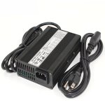
Does anyone by any chance have a schematic for the Wate 180W charger?
I am trying to map the functions of the potentiometers, so I can adjust the parameters of the charger.

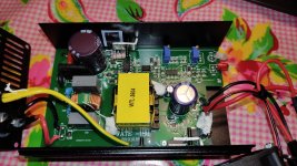
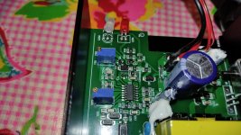
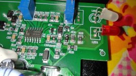
  • VR1 - This one is for adjusting the output voltage. Trial and error with a voltmeter made this one easy to identify.
  • VR2 - This one is missing, and I suspect it could be for adjusting the current limiting, but in mine it seems like R21 have been hand-soldered from the factory with a 30K resistor, so they could leave out VR2.
  • VR3 - I do not know what this one does. Turning it has no effect on either voltage level or current limiting.
I have no idea, what value R21 originally was, or what value VR2 should have had. I would love to hear feedback from someone with a WATE-180 with the VR2 pot in, what values the VR2 and R21 have.

Cheers!
 

Attachments

  • Wate-180.jpg
    Wate-180.jpg
    151.7 KB · Views: 1,079
  • inside1.jpg
    inside1.jpg
    406.6 KB · Views: 1,084
  • inside2.jpg
    inside2.jpg
    370.5 KB · Views: 1,082
  • inside3.jpg
    inside3.jpg
    317.8 KB · Views: 1,080
Just a follow-up, since I decided to reverse engineer the schematic, from the unit I have, and it may interest others.
I only bothered to do the secondary side of the charger, since that is where all adjustments are made. The primary side is not that interesting to me.

So I was able to confirm VR1 is for adjusting voltage output (clockwise lowers Vout), and VR3 is for current limiting (clockwise lowers Imax) - as for VR3 it is not that sensitive, so I had to turn a few times to see an effect. I didn't want to turn it too much at first without at least some knowledge of its purpose.

The hand soldered R21 seems to be what determines what voltage range the charger operates in. It makes sense that it is hand soldered in after production, since the manufacturer probably makes a variety of 180W chargers with different voltage/current ranges, and for a different voltage, they just pop in a different resistor here, and adjust VR1.

The missing VR2 is interesting. I think there is a PCB design error, because it does not make sense to me how Q4 is wired. Collector is grounded, and emitter is left floating, so all of Q4, D3, and R33 does nothing in this charger.

I believe, if Q4 was wired correctly (switch around emitter and collector), then it would have controlled whether or not VR2 is parallel coupled to R20 and VR1, based on the output from IC2-1 (charging/complete). Then VR1 would have been used to set a fallback floating voltage, when charging is complete, and VR2 would have been used to set the actual charging voltage, which is higher than the floating voltage. Essentially a working cut-off function, when charging is complete.

Instead it seems they got the PCB traces wrong, left out VR2 when it didn't work, and now this charger voltage is adjusted by VR1, and there is no cut-off/floating function. Only indication via LED is working, but the charger keeps charging after hitting the low current threshold.

I might even attempt to fix Q4, and see if I can get it working properly with floating voltage. Just need to find a proper value for VR2.
I might also attempt to make the cut-off current adjustable on the inputs on IC2-1. Time will tell :D
 

Attachments

  • Wate-180-schematic_rev1.jpg
    Wate-180-schematic_rev1.jpg
    649.3 KB · Views: 22
Last edited:
Hi! Maybe you drew the primary circuit too :)
After couple of charges, charger blown out. Inside oxidation and debris. Ali sent a new one, which I returned to the customer. I want to repair this. PWM VCC and output not typically wired.
 

Attachments

  • KKK_0355.JPG
    KKK_0355.JPG
    314.4 KB · Views: 13
Привет! Может быть, ты тоже нарисовал первичную цепь?:)
После нескольких зарядок зарядное устройство сгорело. Внутри окисление и мусор. Али прислал новое, которое я вернулся в Китай. Хочу починить это. ШИМ VCC и выходы обычно не подключены.
 
Hi! Thank you for your response. My primary circuit based on LD7575 and also differs from the topic author's version.
 

Attachments

  • KKK_0353.JPG
    2.7 MB · Views: 7
Hi! Thank you for your response. My primary circuit based on LD7575 and also differs from the topic author's version.
if you don't see any problems with the board, you shouldn't start repairing power supplies. it can be really dangerous for your health
 
Back
Top