You are using an out of date browser. It may not display this or other websites correctly.
You should upgrade or use an alternative browser.
You should upgrade or use an alternative browser.
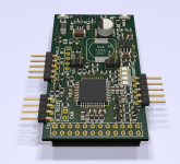
Another SMD lebowski PCB
- Thread starter bobc
- Start date
An in-progress how-to on using these brainboards for controlling the Honda IMA Inverter powerstage is here:
https://www.endless-sphere.com/forums/viewtopic.php?f=30&t=105711
It includes updated / expanded documentation of this brain board, as I find things to correct or add, such as the SMDController.rtf (xls here, zip over there); the original had some typos/etc that appear to have created confusion among builders/users, that then damaged brain boards. The new version should fix that.
kiwifiat
100 W
Pentti M Reku
10 mW
- Joined
- Oct 29, 2020
- Messages
- 28
I would be interested in a readily assembled board.
I can recommend kiwifiats controllers (pieces of art based on Endless Sphere titans), plus the quality and good service! I hope I can contribute to the discussion as soon as I get corona-blocked access to my workplace again with all the needed stuff.
whereswally606
100 kW
Hey Emgee, wondering if I fall into the category of ES titan, at the very most probably just demi-Titan, maybe just a hemi-demi-semi-Titan. Kiwi is definitely a full ES titan, as was Bobc, rest his safety sandal wearing soul.
Good to hear from you.
Good to hear from you.
Pentti M Reku said:I would be interested in a readily assembled board.
X2... but could be interested in assembling one myself.
kiwifiat
100 W
Attached are the updated KiCad files and build instructions. Change the file extension from .txt to .zip.
A big thanks goes to whereswally606 for keeping this project alive. Massive credit to Lebowski for the awesome firmware and design changes to the 15V power supply.
I have the PCB's made at OSHPark in Oregon, USA where you only need to upload the .kicad_pcb file. I have no affiliation with OSHPark, I get a good quality product at a fair price. If you want to plot gerbers you can do that from within KiCad to have the boards made at the manufacturer of your choice. Any questions, fire away.
Attachments
kiwifiat said:Attached are the updated KiCad files and build instructions. Change the file extension from .txt to .zip.
A big thanks goes to whereswally606 for keeping this project alive. Massive credit to Lebowski for the awesome firmware and design changes to the 15V power supply.
I have the PCB's made at OSHPark in Oregon, USA where you only need to upload the .kicad_pcb file. I have no affiliation with OSHPark, I get a good quality product at a fair price. If you want to plot gerbers you can do that from within KiCad to have the boards made at the manufacturer of your choice. Any questions, fire away.
Thanks!
Yes kudos to whereswally606 ando Lebowski
Do I send the PIC to either for the programming?
Cheers
kiwifiat
100 W
squeegee said:Thanks!
Yes kudos to whereswally606 ando Lebowski
Do I send the PIC to either for the programming?
Cheers
Neither, you program the chip yourself with a PicKit2 or 3 via the programming header on the BobC board. The firmware was released by Lebowski a while back as open source.
whereswally606 said:Hey Emgee, wondering if I fall into the category of ES titan, at the very most probably just demi-Titan, maybe just a hemi-demi-semi-Titan. Kiwi is definitely a full ES titan, as was Bobc, rest his safety sandal wearing soul.
Good to hear from you.
Well, I know very well that you deserve your place in the chain of titans! Amazing that Kiwi published the updated hardware and Lebowski released the firmware open source. I'm hoping that the world will be flooded by projects on this basis! Still trying Maybe I can also contribute if I don't continue to destroy my (or your) 'stuff'
I am having trouble understanding what the RS232 circuitry is for. I read that RS232 uses negative voltages = logic high, and positive = logic low. TTL is 0V = logic low, and positive = logic high.
Doesn't the circuit on this board just invert the signals, but are still 0V or 5V, thus not RS-232?
Doesn't the circuit on this board just invert the signals, but are still 0V or 5V, thus not RS-232?
Animalector
10 kW
Rs232 is like -15v to 0V not just inverted logic. Just Dona Google for rs232 interface
Right, RS232 can go down to -15V, and requires at least -3V for logic high.
What I'm wondering is why the signals are called RS232 in the schematic. They look to me like just 0 to 5V signals, albeit inverted with NPN inverters.
What I'm wondering is why the signals are called RS232 in the schematic. They look to me like just 0 to 5V signals, albeit inverted with NPN inverters.
kiwifiat
100 W
Apologies to all that have downloaded the build files. Please do so again. Whilst building a board for member Pentti M Reku I discovered that there was a typo on capacitor C20 which is 4700pf NOT nf. Also the footprint for the LM5017 in the schematic was mirrored. The PCB layout is correct. The file has been updated.
Attachments
Lebowski
10 MW
harrisonh said:Right, RS232 can go down to -15V, and requires at least -3V for logic high.
What I'm wondering is why the signals are called RS232 in the schematic. They look to me like just 0 to 5V signals, albeit inverted with NPN inverters.
Old school 9 pin RS232 give out inverted signals wrt the microcontroller, so that is why I added inverters. I used the bipo schematic because it does not require a chip I dont have. Also, the bipo can deal with +-15V at the input, if necessary. Most 9 pin RS 232 nowadays also accept 5V signals, so this is enough for output to the pc.
If I understand correctly, the controller can talk with most RS232 signals, given they accept 0V-5V.
As my laptop doesn't have RS232, would this be the most straightforward way, using a TTL-USB that allows for inverting both RX and TX, like this?
https://www.mouser.com/ProductDetail/FTDI/TTL-232R-5V?qs=OMDV80DKjRorBEBwmlJ4Pg%3D%3D
Or I could also modify the circuit to bypass the bipolar devices to communicate over normal TTL logic to the TTL-USB?
kiwifiat
100 W
harrisonh said:Or I could also modify the circuit to bypass the bipolar devices to communicate over normal TTL logic to the TTL-USB?
Yes you can. A FTDI TTL to USB adapter connected directly to the DSPIC works.
kiwifiat said:harrisonh said:Or I could also modify the circuit to bypass the bipolar devices to communicate over normal TTL logic to the TTL-USB?
Yes you can. A FTDI TTL to USB adapter connected directly to the DSPIC works.
Thanks! Going to build one up soon
I finished soldering the brain board, but am having issues with RS232.
I programmed the DSPIC through MPLAB X IDE using the programming header.
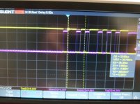
Using a FTDI TTL-USB from Grin for RS232; tried both normal and inverted TTL signals by reprogramming the EEPROM. Checked that it worked with a oscilloscope.
Brain board flashes 2 by 2 when on.
TX pin (after inverter) = 0V.
RESET-> TX pin = 5V
2 by 2 stops flashing
Shouldn't TX be low = 0V during idle?
SETUP-> no change
In Termite, if I try sending a character, the micro doesn't respond. I see the RX signals on the scope though.
[/img]
purple = signal from USB-TTL
yellow = signal at the DSPIC pin
Any idea what could be wrong?
Also, I initially tried an cheap knockoff USB-TTL wired directly to the micro. I didn't realize it was a 3.3V device though. I would get un-readable characters. I then added the inverting BJTs and realized it was only 3.3V, so swapped to the other TTL-USB
[ATTACH type="full" alt="termite.JPG"]283805._xfImport[/ATTACH]
I programmed it after soldering all the components. There were some documents saying to not have any pullups on the programming pins, but the HALL signals have pullups. Could that have caused issues?
I programmed the DSPIC through MPLAB X IDE using the programming header.
Using a FTDI TTL-USB from Grin for RS232; tried both normal and inverted TTL signals by reprogramming the EEPROM. Checked that it worked with a oscilloscope.
Brain board flashes 2 by 2 when on.
TX pin (after inverter) = 0V.
RESET-> TX pin = 5V
2 by 2 stops flashing
Shouldn't TX be low = 0V during idle?
SETUP-> no change
In Termite, if I try sending a character, the micro doesn't respond. I see the RX signals on the scope though.
[/img]

purple = signal from USB-TTL
yellow = signal at the DSPIC pin
Any idea what could be wrong?
Also, I initially tried an cheap knockoff USB-TTL wired directly to the micro. I didn't realize it was a 3.3V device though. I would get un-readable characters. I then added the inverting BJTs and realized it was only 3.3V, so swapped to the other TTL-USB
[ATTACH type="full" alt="termite.JPG"]283805._xfImport[/ATTACH]
I programmed it after soldering all the components. There were some documents saying to not have any pullups on the programming pins, but the HALL signals have pullups. Could that have caused issues?
kiwifiat
100 W
Have you followed the correct proceedure to put the chip into setup mode:
"The chip can be placed in the setup mode by closing the setup switch connecting pin 19
to ground while resetting the chip. Upon entering setup mode a keypress on the PC is
necessary before the chip displays the main setup menu."
I usually press and hold reset, press and hold setup, then release reset, then release setup. I do it in that order because I usually do not want to initiate saving data to the DSPIC.
Oh, I just closed RESET with a jumper. Then closed SETUP with a jumper. I didn't try releasing.
Changed the TTL-USB setup so "invert tx, invert rx" are not checked. (Edit: stopped working after first round of setup. Changed to "invert" and working again.)
Close RESET. Close SETUP. Release RESET. Enter character through termite, and the main menu opened! Thank you!
What procedure would cause data to get saved? And why would you not want it to be saved?
Also, I'm pulling SETUP to ground, which is pin 38, not pin 19. I'm assuming it was carried over from a previous design.
kiwifiat
100 W
harrisonh said:What procedure would cause data to get saved? And why would you not want it to be saved?
Also, I'm pulling SETUP to ground, which is pin 38, not pin 19. I'm assuming it was carried over from a previous design.
The posted schematic shows setup on pin 38, where do you get pin 19 from ?
kiwifiat said:harrisonh said:What procedure would cause data to get saved? And why would you not want it to be saved?
Also, I'm pulling SETUP to ground, which is pin 38, not pin 19. I'm assuming it was carried over from a previous design.
The posted schematic shows setup on pin 38, where do you get pin 19 from ?If you are calibrating HALL sensor offset you press the setup button to save the collected stats to memory, it is all in the manual.
Ah, yes, I understand the "setup" press to save. Thanks.
Edit: Oh. Manual says 19, but schematic is 38. I'm pretty new so don't know when that might have changed..
Similar threads
- Replies
- 64
- Views
- 15,381
- Replies
- 3
- Views
- 2,210
- Replies
- 7
- Views
- 1,974
- Replies
- 97
- Views
- 21,004
- Replies
- 98
- Views
- 15,864


