BMS Schematic help

hardym

100 W
Joined
Jun 7, 2008
Messages
109
Location
San Diego, CA
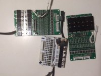
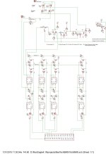
I'm having trouble with a BMS. It seems that many times after hooking up, the BMS seems to be in a "locked up" state, wont charge or discharge. At first I thought that they were DOA, and just broke, but one came back to life. I'd like to understand the problem better, so I created a schematic (attached below). But some of the transistor controller parts don't make any sense. Does anyone have any experience with this type of circuit or have a better schematic?

edit: By the way, I disconnected the cell LV/HV detection lines and the thermal cutoff lines and still get the same problem.
edit2: I updated the schematic to show the load switchs as pfets rather than nfets

The Schematic is similar to one of these:

http://www.bestechpower.com/592v16spcmbmspcbforli-ionli-polymerbatterypack/PCB-D167.html
 

Attachments

  • IMG_3740.JPG
    IMG_3740.JPG
    46.6 KB · Views: 3,017
  • 16chBMSv5.jpg
    16chBMSv5.jpg
    118.8 KB · Views: 2,998
your schematic does not match the parts and circuitry on the D167.

when you say you have disconnected the HVC and the LVC signal lines, what did you do?

none of the LVC and HVC control circuitry makes sense and the labels are not clear. you have n channel mosfets as the shunt balancing transistors but that is not possible if you look at the part in the circuit. it would be reverse biased.
 
your schematic does not match the parts and circuitry on the D167.

It's the best I could do. I think that it's pretty close. If you have more information on the D167 parts that would be great to share.

when you say you have disconnected the HVC and the LVC signal lines, what did you do?
removing the last resistors in series, R25, and R23 on the diagram should eliminate the HVC and LVC from the cells. Removing the transistor next to the thermal sensor effectively takes that out.

none of the LVC and HVC control circuitry makes sense and the labels are not clear. you have n channel mosfets as the shunt balancing transistors but that is not possible if you look at the part in the circuit. it would be reverse biased.

You are correct. Not much makes sense. I wish I had a better schematic of the power mosfet controller section. And, yes, the load switches are probably p-fets. (I didn't pay too much attention to those parts, they seem pretty straightforward. ) I updated the load switches to pfets and reposted. I cant seem to get a good jpeg diagram out of eagle.
 
i don't know what you mean by the terms used like load switches, and i could never follow all the traces in the control section but i agree if you remove the last resistor in the signal string then it defeats the HVC and LVC. i had not been able to see how the themral sensor is wired up because of the silicone putty on top.

but why not go back to your original problem and make the BMS turn on initially. it just had to be a mistake in the wiring initially because they work.

did you test any of the gate voltages for either the HVC or LVC signal line circuitry or base bias?
 
Here's Bestechpower D245 BMS that had me scratching my head recently:
D245.jpg
Connected properly it simply refused to power a small 10-100V LED headlamp. D245 uses the "E-switch" so I made sure that was closed, etc. As last resort I tried to push a charge into the pack, lo & behold, it started working. Works in both directions and the E-switch turns it ON/OFF. OK....

Moral here is that if you're confident connections are good try pushing a charge into the pack and maybe it will start working? Of course, that won't do us much good if the damn thing decides to "need" a charge current to switch ON while out riding.
 
My D245 testing reveals that if/when the balance connectors are unplugged and reconnected the BMS requires a charge current in order to function again. I’m now testing to see if this behavior also applies after the BMS/PCM goes into cell LVC protection mode.
 
usually if the BMS sees LVC, always 2V, and shuts off then it will reset when the cell voltage climbs back above 2.30V.

i am not too familiar with behavior of this design. but from looking at the BMS on slowco's sunthing pack thread you can see the difference in design. the D167 and this one both have the mosfets tied end to end. i think this is how they shoulda designed his.
 
What happened on this D245 (lipo, btw) is that cell LVC (ODDV) shut down after 1 cell hit about 2.9V (which is the spec). Left it sit a few minutes and that cell floated up enough for the BMS to release and turned back ON, by itself. It did this a time or two until the low cell no longer floated up enough to release and the BMS remained OFF.

At this point applying charge current is the only thing I expected to function on the BMS which it did.

Now doing a full charge to see how the HVC side of things behave.
 
ok, lifepo4 on the brain. i wish i could see how the circuit works like he showed in that schematic. especially the transistor on the thermal breaker and the circuit for LVC and HVC. my eyes are so far gone it is almost impossible to see the traces.
 
Boy, do these things get hard to follow what’s happening... I don’t have enough logging or externally powered meters to know 100% what happened on the HVC charge cycle but I’ll try to explain.

This is a pretty well balanced pack and it appears the HVC cut-off based only on the 67.2V pack voltage, 16S Li-ion and I don’t believe any cell ever hit HVC 4.25V. All the cells seemed to be hovering around 4.20-4.22V/cell when I checked immediately following charge termination.

What’s confounding to me is that the charger input terminated although the BMS continued to power a small LED meter paralleled on the output. In other words, it no longer passed higher potential charge current to the battery but still allowed load current to flow from the battery.

Things got really weird when I unplugged some 4S groups on the balance channels to test for protection in the event of a failed sense wire and/or 0V cells. In every case the BMS shutdown. But when reconnected, it required that brief shot of charge current before it would again power any load.

That seems an odd thing to potentially deal with out on the road and might also be related to the “locked-up” condition noted in OP?

The more I learn the less I know….

But I do know I like the E-switch once the D245 BMS is unlocked from it’s ZOMBIE state. I've hacked the Temp sensor switch before on D167's but it only turned BMS OFF and still needed to cycle P connection to turn it back ON. The D245 E-switch actually allows the BMS to also serve as a pack ON/OFF switch. Useful...
 
art mentioned he had the same problem using the switch on the thermal breaker. i don't use them so i am kinda limited. his schematic may offer clues so i will try to find one somewhere and look at it more closely.

it sounds like you did have one cell go to the HVC so you have to drain charge down to the reset voltage.
 
Gonna fab some parallel balance cables in order to log individual cells with a couple CellLog 8S. That may reveal some useful HVC/LVC behavior data.
 
yep. i hang three cellogs on my 21S lipo pack and have the alarm set to 4.22V so i have a good idea of where it is during charge. then it will alarm at 2.90V on the discharge so i know when to back off the throttle just by listening for the alarm.
 
ok, i can finally confirm the schematic for the thermal breaker and the pnp transistor. as i understand the circuit, that transistor is turned on by the base current from that resistor divider bridge when the breaker is closed. when it opens then the base must have to rise in voltage to turn of the pnp transistor. not sure how that happens if his circuit does as it should, but i confirmed the layout. the little 12V circle is the through hole in the corner where the trace turns. that is the emitter of the pnp transistor. but where he has the ground on the end of 225 that is actually attached to the LVC signal line. so when the signal line goes high it will bring the base of that pnp transistor high and that turns it off so there is no current to those diodes.

so to hack the thermal breaker circuit in order to use it for an on/off switch for the BMS you would connect the emitter of the transistor to the base through the switch, by lifting the transistor and soldering the wires to the DIP switch onto the traces used by the transistor. i will do that yet. see if i can turn the BMS on and off.

so next i am gonna follow the HVC and LVC circuit to see how it works too. the trace leading away from the collector ends up going through a 685 surface mount to some diodes. not sure what i am looking at there. but not this circuit in the schematic yet so maybe it is a different version. gotta look at it for awhile.

while following the diodes i realized the two empty holes out in the middle are for a kill switch on the battery. it brings the voltage onto the LVC signal line at the very top and that turns off the mosfets immediately when you connect the two through holes there. way cool to know. a NO switch will turn off the mosfets when closed. like and interlock or temperature sensor input.

you must have some experience with analyzing circuits from the traces to draw that schematic. kudoes, etc.
 
Messed around with a paralleled JST cable. What we have here is final minutes of a charge where it appears the BMS detected high cell voltage 4.24V and shutdown.

Without a ton more adapter wiring it’s difficult to connect a CellLog on channel 9 so I’m just going with #1-8. Will probably get around to #9-16 but this is where it’s at for today.
D245Ta.jpgFullSizeRender.jpg

It should be noted BestechPower D140/D245 BMS/PCM use very similar JST connector as those found on RC Lipo. MAJOR DIFFERENCE is reverse polarity. Easy enough to deal with on CellLog, etc. But just be aware of this if you use RC gear.

D167's use a much narrower JST type connector so those are more of a hassle.
 
you can buy plugs with the 2mm spacing instead of the 2.54mm spacing of the JST plugs on ebay.

also you can solder your own connector to the traces where the sense wire plug is soldered to the pcb so you have a parallel set of sense wires and you can use your cellogs on that plug.
 
This D245 doesn't have the large pads to solder like the D167 and probably others so I refrained from any taps off PCB.

Pretty cool to see it behave as spec'd on discharge, charge graph:

I've got enough connectors to fill out a 2nd adapter cable and I've got 2 CellLog 8S, just gotta hack #8 (pos+) for #9 (neg-) on the current adapter.
 
how did you record this? do you use the 8S type cellog and then download the data from it?

interesting how the two lowest cells at the end of discharge started out just like the others and the blue one which was low at the beginning did not drop out with them.
 
Yes, 8S CellLog captures the voltage graph then render it on a computer. Cool to see the minor variations in IR, eh?

Here's the entire cycle if you're curious and the OP doesn't mind?

Keep in mind this is just hobby grade gear but it's proven to be reasonably accurate.

I started another thread, adding some of the CA screenshots to accompany the log graphs over here:
http://endless-sphere.com/forums/viewtopic.php?f=2&t=66791
 
Back
Top