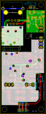
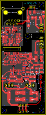
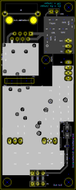
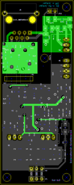
15A gate with negative bias and differential PWM input

zombiess

10 MW
Joined
Jan 31, 2011
Messages
3,048
Location
Oklahoma City
I started working on this gate driver design about 2 weeks ago. I've been working to improve on the previous and now I'm starting to experiment a little. This gate drive is being designed to drive a large bank of parallel MOSFETs for a controller idea I'm testing out. It's going to be in what could be considered a harsh EMI environment.

Right now this is just a draft, but I'm hoping to have the boards produced soon so that I may start slaving away with the soldering gear and some tweezers. As much as I want to rush into building this, I know better.

I'm trying to get a part justification write up done to explain things that might not be obvious. Right now only 1/2 of the differential setup is visible, the other side is placed on the controller board.

The PWM signal and the fault out from the gate drive and +5v and +24V are being carried over CAT6 shielded twisted pair. That provides 8 conductors and one shield.
2 for PWM (differential)
2 for Fault (differential)
2 for +24V
2 for +5

Since there are 6 gate drivers for a 3 phase setup, there will be six CAT6 cables running to the controller. I anticipate the length being ~1m, maybe 0.5m.

The reason for differential signaling is it has very high CMRR. CMRR = Common Mode Rejection Ratio. I chose to go with an RS485 driver chip as I believe it fit the need well and comes in a neat little package requiring very few additional parts. I added some TVS diodes to improve the static sensitivity, because the cables will be handled more often than I would like.

Posted up are KiCAD files and PDFs of the board layout and schematic. Sorry about the super thin traces in the PDFs, that's a KiCAD bug. Some of the voltage call outs are incorrect as I used specific vs generic names, then changed the voltage converter from 15V to 12V... my bad, need to edit that.

Post up questions if you got them.
 

Attachments

  • Gate Driver 1-5 Layout.pdf
    105.5 KB · Views: 68
  • Gate Driver 1-5 Schematic.pdf
    90.8 KB · Views: 94
Preliminary parts choice explanation and justification. I still need to do the output parts, but this is the detailed more difficult stuff to understand.

DC101 - PQMC3-D24-D12-S - 3W DC/DC Converter 24V DC supply, +12V/-12V output @ +/- 125mA. Power supply for gate driver.
Rating - 3W was chosen because the gate drive has maximum switching freq of 30kHz. The maximum Qg encountered (without the addition of G-S capacitance) is 75mA which translates to 1800mW at +/- 12V. At 20kHz operation the DC-DC needs to supply 50mA or 1200mW.

Gate drive average current Idrive = Qg * fsw
2500nC * 30000Hz = 75mA

Gate drive average power Pdrive = Idrive * delta_gdV
75mA * 24V = 1798mW
Idrive = 75mA
delta_gdV = 24V, |-12| + 12

C101 - 10uF XR7 50V - SM1206 - Input filter capacitor (value chosen following DC101 datasheet)

L101 - 6.8uH - SM1206 - Differential choke (value chosen following DC101 datasheet)

C102 - 1uF XR7 50V - SM1206 - Bypass/Filter cap (value chosen following DC101 datasheet)

J101, C104, D101, R101 - DO NOT POPULATE - See DC101 datasheet for values if this feature will be utilized. These components make up a circuit to enable/disable DC101.

L102, L103 - 6.8uH - SM1206 - differential choke, noise reduction (value chosen following DC101 datasheet)

C103, C105 100uF 25V - SM1206 - Output filter capacitor (value chosen following DC101 datasheet)

R102, R103 - 1k Ohms 0.25W - SM1206 - current limiting resistor for D102 & D103, expected dissipation 0.08W. 0.1W resistors do not provide enough overhead to handle temperature fluctuations.

D102, D103 - LED - SM1210 - 3.3V forward voltage drop. These LED's current limited from 8-10mA are used to ensure minimum load requirement is met for DC101's output and provide visual indication that DC101 is powered. DC101 calls for a minimum of 5% load to maintain regulation spec. DC101's output is 125mA, 5% of 125mA = 6.25mA.

J1 - 0855055113 - RJ45 Jack with shield - carries +24V for DC101 and +5V for signaling.

TVS1, TVS2 - PSM712-LF-T7- SOT-23T - 7V TVS Diode, static/overvoltage input protection.

R11, R17 - 100 Ohms 0.1W - SM0805 - RS485 data bus termination.

U3 - LTC2863-1 - SO8E - RS485 Transceiver which is used in full duplex mode to receive PWM information and transmit back fault signaling. All transmissions are done differentially to improve CMRR. This device incorporates a failsafe operation which causes the output to be a logic 1 if the inputs are shorted, left open or terminated but not drive for more than 3us.

R10 - 2.2k Ohms 0.1W - SM0805 - Reduces base emitter current. A BT2907 has an hFE of 75V @ 0.1mA. The LED in the 6N137 is driven with 15mA (Set by R3). Base current needs to be higher than 15mA/75 = 0.2mA. Desired base current = 10x 0.2mA = 2mA. On state emitter-collector voltage 0.4V.

Current through LED = (5V - (0.4V + 1.9V)) / 180 Ohms = 15mA
Current through base resistor = (5V - (0.7V + 0.4)) / 2.2k Ohms = 1.8mA = ~2mA
Wattage = (5V - (0.7V+ 0.4V)) * 1.8 mA = 0.005W

Q4 - BT2907 - SOT23-3 - acts as a switch to pass higher current from the 5V supply. Base signal supplied by U3 is 5mA. Q4 is off when the base is high and on when the base is low. The LTC2863-1 IC outputs a high state when it is idle or a failure is detected.

R3 - 180 Ohms 0.1W - SM0805 - current limiting resistor for LED in IC1.
Desired LED Voltage = 1.9V and current = 15mA

Current through LED = (5V - (0.4V + 1.9V) )/ 180 Ohms = 15mA
Wattage = (5V - (0.4V + 1.9V) ) * 15mA = 0.04W

R5 - 22k Ohms 0.1W - SM0805 - Q4 pull up resistor to ensure state of Q4 is off if something in the signal chain before it fails. The value of 22k Ohms was chosen because it is 10x the base resistor and is standard practice.

IC1, IC2 - 6N137 - S08N - Optical isolator with open collector output. When LED is on, output is low, LED off = output high. This matches the TD350E's truth table which is active low. If the LED is off due to failure IC1/IC2 output a high signal keeping the TD350E turned off preventing a possible shoot through condition.

R13 - 4.7k Ohms 0.1W - SM0805 - pulls output high which means no fault detected. If there was a failure of the +5V from the controller board, the signal would go low triggering software fault detection at the controller side.

C9 - 100nF - SM0805 - bypass capacitor for IC2 and U3

C17 - 10nF - SM0805 - bypass capacitor for IC2 and U3

U1 - MC78L05ACH - SOT-89 - 5V 0.1A positive voltage regulator. Supplies 5V for IC1.

C4 - 100nF - SM0805 - bypass capacitor for IC1 and U1

C3 - 10nF - SM0805 - bypass capacitor for IC1 and U1

C6 - 47pF - SM0805 - ??

D4 - 5.1V Zener - SOD323 - protects input of U2.
D4 must have a zener current < 12V / 4.7k = 2.5mA.

R4 - 4.7k Ohms 0.1W - SM0805 - pulls input of U2 high forcing an off state since the gate driver is active low. D4 prevents the +12V power from exceeding the 5.5V input of U2.

R14 - 4.7k Ohms 0.1W - SM0805 - LED current limiting resistor.

(5V - 1.9V) / 330 Ohms = 9.4mA

2 Level Turn Off
The two-level turn-off is used to increase the reliability of the application.
During turn-off, gate voltage can be reduced to a programmable level in order to reduce the
current (in the event of overcurrent).

Notes on component choices - Roff from 10kΩ to 20kΩ, and Coff from 100pF to 330pF, providing
a range of delay from approximately 0.7 to 4.6 microseconds.

Coff Calculation
tA[μs] = 0.7 x Roff[KΩ] x Coff[nF]

The following two components set the 2 level turn off delay of 0.33us
R12 - 4.7k Ohms 0.1W - SM0805 - Roff
C8 - 100pF - SM0805 - Coff

The following two components set the 2 level turn off voltage
R12 - 4.7k Ohms 0.1W - SM0805
D6 - 7.5V Zener - SOD323 - sets 2 level turn off voltage. IRFP4568 has a miller plateau of ~6.5V.
 
awesome man! love reading your technical posts!

small remark about the PCB, it's good practice to avoid corners less than 90 degrees, because there is a bigger chance of unwanted copper leaving behind in the etching process. (probably not even a problem, as you have a large clearance between traces)
 
just some feedback for schematic (i didn't look at layout)

power supply minimum load. during bentch test (or by analysis), you should see if you have naturally 5% load without the LEDs and if so you can pull them off if you want slightly higher efficiency. on cheap power supplies though, probably its best to leave them on to ensure stability even if your min load is 10%.

LTC2863-1,the failure mode is output logic one? would such a mode cause your mosfet to be conducting or OFF?

transistor at opto input IC1. make sure this transistor is going to produce the square waves cleanly at the frequency you want (spice simulation).

differential driver.. i gotta read this datasheet in detail. the device is differential driver, but your layout is not. could be that's fine for the device to work, just doesn't look "differential" to me, so i'm going to go read on this more and get back to you. for true differentially driven noise immunity, the input to pwm opto (IC1 for example) has to be **driven** in reverse in the OFF state. that's what i was looking for in your schematic and i didn't immediately see how that could be done. oh... maybe you are just trying to make the communication path differential, not the actual pwm opto (i.e. if you had a really long distance between brain board and gate driver board?). ya you could do it this way.. still though i would be more inclined to use the shielded cable that you have, grounded on one end, and then differentially drive all the way to the opto input (rather than stop at the driver chip you have).

you can improve the noise immunity further by incorporating hardware level interlock between upper & lower drives. know what i mean? this is an H-bridge topology where your critical failure is shoot-through. your PWM should be supplied in a half-bridge mentality rather than per mosfet way. think about driving the phase leg rather than the individual mosfet and how your pwm can be driven to both in such a way to make sure one is driven ON while other is *hardware forced* off.

my feeling is you don't really need to differentially drive the fault feedback because the time of response requirement is low (1ms). you could heavily filter instead. this is assuming your gate drive IC has built in fault protection which it does. i know your differential IC has two channels so you might as well use it.. ok, but, let's say you where driving the phase leg instead of per mosfet and assuming you could find a differential IC that had two channels but both channels face same direction. use those two for pwm and then just wire back the fault signal (with heavy filter).

make sure your pwm cable with its ether net jack style connection is suitable for high vibration. you don't want lose connections here at all!

double check your opto datasheet, make sure this opto has very good CMRR. i think i gave you a guideline of what values to look for here. also, and this is not always on the datasheet, look for very very low input-to-output parasitic cap value, should be in the 10pF range.

on your boost stage, your caps are shown in wrong order. since the flow of current from cap is through the boost stage transistor (not the IC) then your smallest nF cap should be closest to the transistor and largest is farthest away. electrically it makes no difference, but if you place on your schematic in this way it will imply that is how it is layed out on the board (smallest cap is closest to the transistor). one of these caps would be placed near the gate drive IC bypass, looks like u chose C7 for that. u might consider adding a 10nF between C7 and gate drive IC since this IC does do switching of current (drives boost stage) so there will be multi frequency noise.

-15V off is way overkill for a mosfet, even in high noise environment. also be careful to read all your datasheets because now you are talking about a 30V differential voltage and not all parts can handle that much (i forget how much the gate drive IC is rated for).

your PWM opto input does not have a defined state on power up (or loss of power).

what is the behaviour of U3 at initial power up? what is behaviour of your Q4 transistor stage at power up? remember, andy screw up here or any noise coupling at startup here may cause catastrophic failure (shoot-through). your gate drive IC, TD350, one of the reasons i like it is that it has good startup measures (low voltage lockout).

i don't understand your U1 linear voltage regulator output, you tie the output to +15V supply? or maybe you mean U1 intput should be tied to +15V?

IC1 & IC2, you sure pins 7/8 should be tied together?

still you put D1 and D2 in wrong spot. i know you have your appnote showing that your way is acceptable, but i disagree. guess we .. still .. have to agree to disagree on this :p
 
This type of isolators is usually very easy to use instead of optos:

http://www.silabs.com/Support%20Documents/TechnicalDocs/Si841x-2x.pdf

I don't know if it suites or app better or not than optos, but the general specs look good (1 or 2pF in-to-out @ 1MHz depending on package, HighHopes).
I've used similar chip but for I2C and from AnalogDevices, and I'm totally sold.
 
Njay said:
This type of isolators is usually very easy to use instead of optos:

http://www.silabs.com/Support%20Documents/TechnicalDocs/Si841x-2x.pdf

I don't know if it suites or app better or not than optos, but the general specs look good (1 or 2pF in-to-out @ 1MHz depending on package, HighHopes).
I've used similar chip but for I2C and from AnalogDevices, and I'm totally sold.

Thank you for the part Njay. I'm just starting to branch out and experiment with different design options now that I have built 2 working setups.

HighHopes, are there any caveats to this type of isolator vs a opto coupler?
 
HighHopes said:
power supply minimum load. during bentch test (or by analysis), you should see if you have naturally 5% load without the LEDs and if so you can pull them off if you want slightly higher efficiency. on cheap power supplies though, probably its best to leave them on to ensure stability even if your min load is 10%.

LEDs guarantee it will meet minimum load while showing that devices are powered, but more importantly I chose red, white and blue... 'murica! I'll probably have to tweak R values to get them all the same brightness if I'm feeling fancy :mrgreen:

I'm choosing a part by CUI. While I'm not very familiar with the company reputation, I'm more comfortable with them for this project after reading the spec sheets. The converter is also regulated vs unregulated but comes with an added bonus of having it's output rated for a short condition. I have managed to kill 2 of the cheapo units I've used in the past by shorting them for < 2 seconds during testing. CUI also provide a good details on how to implement the device and more importantly, it comes in a foot print I wanted to help keep the driver small. Keeping full features on a gate drive while staying compact is a challenging.

LTC2863-1,the failure mode is output logic one? would such a mode cause your mosfet to be conducting or OFF?

Handled by Q4 - see description above

transistor at opto input IC1. make sure this transistor is going to produce the square waves cleanly at the frequency you want (spice simulation)
.

Simulation looked good, I had some other concerns so I took the time to simulate it.

differential driver.. i gotta read this datasheet in detail. the device is differential driver, but your layout is not. could be that's fine for the device to work, just doesn't look "differential" to me, so i'm going to go read on this more and get back to you. for true differentially driven noise immunity, the input to pwm opto (IC1 for example) has to be **driven** in reverse in the OFF state. that's what i was looking for in your schematic and i didn't immediately see how that could be done. oh... maybe you are just trying to make the communication path differential, not the actual pwm opto (i.e. if you had a really long distance between brain board and gate driver board?). ya you could do it this way.. still though i would be more inclined to use the shielded cable that you have, grounded on one end, and then differentially drive all the way to the opto input (rather than stop at the driver chip you have).

I'm debating changing this to the differential design you are talking about and combining 2 drivers onto a single PCB and only needing a single wire run to it. This is a different type where it's driving only one side of the half bridge. I have a specific reason in mind for doing it this way though.

you can improve the noise immunity further by incorporating hardware level interlock between upper & lower drives. know what i mean? this is an H-bridge topology where your critical failure is shoot-through. your PWM should be supplied in a half-bridge mentality rather than per mosfet way. think about driving the phase leg rather than the individual mosfet and how your pwm can be driven to both in such a way to make sure one is driven ON while other is *hardware forced* off.

Care to elaborate further?

my feeling is you don't really need to differentially drive the fault feedback because the time of response requirement is low (1ms). you could heavily filter instead. this is assuming your gate drive IC has built in fault protection which it does. i know your differential IC has two channels so you might as well use it.. ok, but, let's say you where driving the phase leg instead of per mosfet and assuming you could find a differential IC that had two channels but both channels face same direction. use those two for pwm and then just wire back the fault signal (with heavy filter).

The differential going both direction was to minimize the chance of a false fault from noise.

make sure your pwm cable with its ether net jack style connection is suitable for high vibration. you don't want lose connections here at all!

This is something that concerned me and I debated on this design choice, but I decided to do with it because this is mostly going to be used in a lab type environment. My driver and power stage are modular. I'll probably hot glue or epoxy the gate driver side connections. I anticipate a cable length of 1m.

double check your opto datasheet, make sure this opto has very good CMRR. i think i gave you a guideline of what values to look for here. also, and this is not always on the datasheet, look for very very low input-to-output parasitic cap value, should be in the 10pF range.

Min CMRR = 5000:1, typical=10,000:1
It's 0.6pF, but thank you for the reminder! I forgot about this rule.

on your boost stage, your caps are shown in wrong order. since the flow of current from cap is through the boost stage transistor (not the IC) then your smallest nF cap should be closest to the transistor and largest is farthest away. electrically it makes no difference, but if you place on your schematic in this way it will imply that is how it is layed out on the board (smallest cap is closest to the transistor). one of these caps would be placed near the gate drive IC bypass, looks like u chose C7 for that. u might consider adding a 10nF between C7 and gate drive IC since this IC does do switching of current (drives boost stage) so there will be multi frequency noise.

I didn't realize I had them backwards, but now that you write it out it makes more sense. Gonna swap that around. I'll add on the 10nF as you mention as well.


-15V off is way overkill for a mosfet, even in high noise environment. also be careful to read all your datasheets because now you are talking about a 30V differential voltage and not all parts can handle that much (i forget how much the gate drive IC is rated for).

I'm actually going -12V off since that's my supply. I need to change the schematic symbol. -12 is still over kill, but it's easy to get a 3W dual rail 12V DC/DC.

your PWM opto input does not have a defined state on power up (or loss of power).

You got me on that one, I missed it, thanks.

what is the behaviour of U3 at initial power up? what is behaviour of your Q4 transistor stage at power up? remember, andy screw up here or any noise coupling at startup here may cause catastrophic failure (shoot-through). your gate drive IC, TD350, one of the reasons i like it is that it has good startup measures (low voltage lockout).

U3 goes to a logic 1 at power up which is the idle state. Q4 is pulled high by R5 which is 22k, this keeps the LED in the off state during power up. The default to a logic 1 state is why I chose a PNP part vs an NPN part.

i don't understand your U1 linear voltage regulator output, you tie the output to +15V supply? or maybe you mean U1 intput should be tied to +15V?

I think you read the schematic incorrectly because I have the regulator flipped. Not sure what the best practice is here for schematic drawing, I'm still learning what is good practice. I hope they are becoming more readable. I'd like to switch packages away from KiCAD as it lacks some basic features I need, but it is open and easily accessible to many.

IC1 & IC2, you sure pins 7/8 should be tied together?

Yes, pin 8 is Vcc and pin 7 is the enable pin which must be pulled high for the 6N137 to operate. But now that I read this again to answer your question, I'm thinking it might be a good idea to have the fault out of the TD350E pull this pin low. This would satisfy the hardware PWM shut down criteria. I could then add on an RC timer to create a short blanking period which might allow a recoverable fault to clear, maybe ~500us? 500us would miss 15 pulses at 30kHz PWM and 6 pulses at 12kHz. The software shut off would still be in the loop, but I would recode it to only shut down in the event of x faults/period. I think I just talked myself into this :D It's going to make it more robust.

still you put D1 and D2 in wrong spot. i know you have your appnote showing that your way is acceptable, but i disagree. guess we .. still .. have to agree to disagree on this :p

I've swapped them to the "proper way", no argument, I just knew it worked way on the bench following the app note. As you mentioned to me previously, once you know something works you become reluctant to change it :p
 
zombiess said:
Njay said:
This type of isolators is usually very easy to use instead of optos:

http://www.silabs.com/Support%20Documents/TechnicalDocs/Si841x-2x.pdf

ahhhH!! i hate digital isolators :(
this kind of part is more suitable to low voltage application and with one side NOT switching reference 600V in 200ns. the "digital" part of the digital isolator is very sensitive. i think the intent of that part is to separate grounds for digital communication application. i didnt read the datsheet in full (i closed soon as i say "digital isolator") but other digital isolator datasheets i have read do not have ability to maintain a DC output. i know we "never" have that in PWM application, but once you get to more advanced stuff of high performance motor drive you will appreciate that feature (right now, after 2 years, we're just finishing up how the gate driver needs to be designed for it to be functional AND reliable, we haven't touched the system level stuff yet).
 
The converter is also regulated vs unregulated
for gate driver power supply prefer to have unregulated. for regulated there has to be some feedback on the powersupply from secondary to primary so it can make its control. in gate driver application the reference on the secondary side switches 600V in 200ns (or whatever) and that will wreak havoc on the control bits of the power supply and provide an avenue for noise to travel from secondary to primary. if its unregulated then you might not get the +15V -12V, maybe +/-10% but your application is not sensitive to variation so its worth the trade-off. for your design i'd say its ok to use regulated because your power level is still low enough.. but you said "high noise" environment. if you mean that your product is the source of the high noise, then you have to design for that which means your are obligated to use unregulated power supply (don't blame me, its your rule!).

you can improve the noise immunity further by incorporating hardware level interlock between upper & lower drives. know what i mean? this is an H-bridge topology where your critical failure is shoot-through. your PWM should be supplied in a half-bridge mentality rather than per mosfet way. think about driving the phase leg rather than the individual mosfet and how your pwm can be driven to both in such a way to make sure one is driven ON while other is *hardware forced* off.
Care to elaborate further?
check my EV controller design thread on ivan's forumn. i used a PWM interlock via AND logic chip. other way to do it is the current that flows through your opto's input LED has to be the same current that flows in REVERSE direction of adjacent opto (i.e. through an anti-parallel diode external to the part) thus reverse biasing the input. you need true differential drive to do this but its rock solid way (probably better than AND chip method). it takes a lot of current though, like 5 to10mA. <-- this is a bit of the "advanced" stuff we're starting to get into so that's exciting. progress!

The differential going both direction was to minimize the chance of a false fault from noise.
no doubt, i was just making the argument that you don't need that. fault signal can be filtered heavily instead to remove noise and significantly lower chance of nuisance trip. the PWM theoretically you could do the same but in reality you can not because the group delay of such heavy filter would kill your control stability.

Min CMRR = 5000:1, typical=10,000:1
huh.. i only ever seen this parameter described as so many kV/uS. i like the kV/uS datasheets because i know how many of this unit my mosfet will create since i know the switch time and the DC bus voltage thus i know quite clearly if the opto is good or not. 10000:1, how do i relate this to my gate driver, how do i know if that's good enough?

It's 0.6pF, but thank you for the reminder! I forgot about this rule.
i wrote 10pf above, this is for total gate driver input to output. so look at all your things that sit on the interface of the isolated grounds which for your design is one power supply and two optos. add up the total input to output parasitic cap, not allowed to be more than 10pF. so you have 2 x 0.6pF + whatever the power supply is (i'm going to say its probably in the 20 to 30pf range). for "high noise" immunity, no single part is allowed to be higher than 5pF ideal (10pf max acceptable). something like that, its just a guideline don't go nutz on me. the number comes from your mosfet switch volts per second (DC bus in switch transistion time which might be 100ns or so). use formula i = C*dv/dt where dv/dt is your mosfet Volts per Second and C is your design rule of 10pF (or whatever numer you want to use) and i is your injected current. that injected current could be on ANY of the brain to gate driver interface regions. so lets say your opto input had 330 ohm in series wiht the LED (a common value). now you inject this nosie current via the opto's case (parasticc cap) onto that PCB trace and multiple this noise current by the series resistance of 330ohm and you get a voltage. what will that voltage do? if nothing then 10pF design rule was good choice, if something 10pF is too high.
 
actually.. that's a good thing to clear up. when u say high noise environment do you mean your product has to survive in environment where the noise is extrnal (some other source) or your inverter is the source of the noise. i'm assuming you mean your product is the source. if so, do you plan to make two solutions, the first being your product has to work (functional + reliable) plus it also has to NOT kill other products by blasting it with nosie (i.e. you have to shield somehow your product so its conducted/radiated emissions doesn't disturb other things like your cell phone or other car electronics).
 
This inverter has the potential to be quite noisey. It could be switching peak currents > 1kA @ 120V. I am trying to slow down the switch timestimes from what I have done in the past. I'll have a better idea once I start bench testing the output stage with some single / double pulse tests.

I am in the process of acquiring a rogowski coil to help analyze the power stage layout. This could lead to a more interesting gate drive we talked about previously. I need to get my hands dirty and "get a feel" for what is happening.

The rules are getting more interesting now. Thanks for the above explanations, now I have more things to check + some design changes like the pwm input.
 
This is v1.5.1
View attachment Gate Driver 1-5-1 Schematic.pdf.pdf

Some small changes have been made. R20 was added to keep the opto LED in a known state at all times, some 10nF bypass caps added, cleaned up the 5V regulator circuit. I also re-orderd the boost stage caps to the proper order.

I also changed out the regulated DC-DC for a unregulated version which output +15V/-8V at 100mA/80mA. This is a 2W rated unit which might limit maximum switching freq. I've calculated that I require 1723mW @ 30kHz. At max freq this is ~14% margin which is not much. I plan to operate at 21kHz so there is headroom available as the power demand is only 1200mW.

This DC-DC has 6.6pF of parasitic capacitance + each opto at 0.6pF for a total of 7.8pF :D


View attachment 1
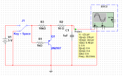
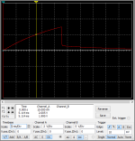
Biggest change is the addtion of R18, R19, R21, Q5 and C16. This circuit forms a self resetting hardware PWM interrupt. The RC components chosen provide a minimum 0-2V time of 5.1ms (not sure how long to make this :? ). C16, a 1uF capacitor charges from pin 3 of the TD350E through R18 & R21, 10k and 15 ohm resistors. The TD350E fault output is high during normal operation and low during a fault. Q5 is open when it's base is high which is normal operation. When a fault occurs, the TD350E output goes low < 1.0V, this pulls the base of Q5 low causing it to conduct. C16 discharges through R21 which limits the peak current to 333mA since Q5 has a max of 600mA. On the next falling edge of PWM the fault output is reset back to 5V. This makes the base of Q5 high turning it off and allowing C16 to charge to 5V through R18+R21. The minimum enable voltage for IC1 is 2.0V.

This fault circuit works in parallel with the PIC error handling micro I use to stop the PWM at the brain side. It will be programmed to fault on the 2nd error. This should prevent false triggering of the secondary fault detection which will shut down and latch the PWM input off until it is cleared by a manual power cycle.

This is a simulation of the circuit operation created with Multisim
sim.png
pulse.png
 
Back
Top