Hi all, long time listener first time caller.
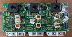
I recently acquired a Infineon Hybridpack 2 IGBT set and driver board directly pulled from a full motor controller/inverter for automotive applications. Specifically, I determined it is from a Chinese company that makes inverters for cars and busses, and based on some other sleuthing this was likely an engineering sample for an inverter they were developing that could do 100-200kW. Picture of the full board attached below. It is difficult to photograph because of the conformal coating being so shiny. It looks very 'reference design'-ish to me, so if anyone recognizes the full topology, that would be great. The wires you see coming off it are from me, there just to probe/power things.

These IGBT part is an Infineon Hybridpack 2 FS800R07A2E3
Link to datasheet: https://www.galco.com/techdoc/eupc/fs800r07a2e3_dat.pdf
As you can see, these are pretty serious bits of kit. From what I understand, almost this exact Hybridpack IGBT is used in the Chevy Bolt.
I'm interested in reverse engineering this guy to use with my own logic board (something VESC-based maybe, in effort to make my own cheap 'Axiom'-controller). No specific application, just as an exercise. I've run up against a few roadblocks and thus figured I'd start cataloging my effort here and just to share the information. Also figured some people may be interested in how these are built.
What I have determined thus far:
This board is completely analog/dumb- that is, there is no MCU/FPGA/CLPD's. There are op-amps / comparators, there are driver IC's, isolation transformers, a flip flop IC, so other isolation ICs, along with some components on the backside that I unfortunately cannot see without desoldering the board from the IGBT's, but look to be voltage regulators. So this was very good news- the PWM signals from a seperate logic board most likely must pass to this board directly.
The main components of the board seem to stem from six individual isolated gate driver sections, all of which use:
ACPL-32JT
"Automotive 2.5 Amp Gate Drive Optocoupler with Integrated Flyback Controller for Isolated DC-DC Converter, Integrated IGBT Desat Overcurrent Sensing, Miller Current Clamping and UVLO Feedback"
Datasheet: https://docs.broadcom.com/doc/AV02-4256EN
Current sensing per phase is done with the HC5F900-S - an analog 0-5v output sensor, with each one being conditioned with some basic analog op-amp circuitry.
There are two IC's that straddle the isolated zone that are labeled as:
ACPL-C87BT
Broadcom Automotive High Precision DC Voltage Isolation Sensor
Datasheet: https://docs.broadcom.com/doc/AV02-3564EN
Which I take it are for the HV DC measurement as well as maybe phase voltage measurement (although there are only two? and I see none of that package on the backside of the board)
There is one logic IC, which is a SN74AHCT74, which is a Dual Positive-Edge-Triggered D-Type Flip-Flops With Clear and Preset - I have a feeling this is a catch-all fault mode latch, summing potential fault signals from the ACPL-32JT's? I cannot trace it out however.
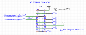
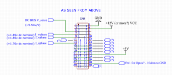
There are only two power rails that I can see feed from the main connector- a +12V and a +5V. The 12V at some point drives a boost converter that raises that up to 16-18V for the ACPL-32JT opto driver IC's. I confirm that when I power up the 12v and 5v rails together, all the comparator/op-amps get their 5v rail, and the ACPL-32JT's all get powered by 18v (or around there).
The only connector on the entire board is a single 30-pin connector, and most of the pins on that connector are ganged in pairs, to the point that I think only 12 pins total can be used for current sensing/voltage sensing/fault detect/igbt temps/the PWM.
Unfortunately that is where I have stopped. I don't have good desoldering equip, not good enough to cleanly desolder the board from the IGBT's, and thus can't quite see what is on the other side (looks like mostly passives and more comparators, maybe a power regulator/boost IC and some 6 pin sot packages.
I can't quite figure out how to trace everything thru from the driver IC's to the main connector. The driver IC's look to have an anode and cathode connection to the LED that drives the opto-coupled connection, and I assume this would be the direct input point for the 6 hi/lo PWM signals for motor control. However, there is obviously some circuitry driving those inputs, and something I can't trace out easily to the connector. I've tried to trace out the current sensors' analog outputs to the main connector, as for sure it would have all 3 current readings as analog voltages present on 3 pints of the main connector, but I can't find them. I thought about running a loop of wire through each one and passing a large sinusoid of current thru the loop and scan the pins for that waveform present as a voltage with a scope, but I didn't get too far with that (need to build something that can drive more current to look for changes, the full scale output of those sensors can read hundreds of amps)
Anyone have any advice on going further... Short of desoldering and x-raying the board? Any tricks, anything you see? It has been so hard to try and trace individual traces, due to not having access to the back of the board and due to the conformal coating on everything.
I recently acquired a Infineon Hybridpack 2 IGBT set and driver board directly pulled from a full motor controller/inverter for automotive applications. Specifically, I determined it is from a Chinese company that makes inverters for cars and busses, and based on some other sleuthing this was likely an engineering sample for an inverter they were developing that could do 100-200kW. Picture of the full board attached below. It is difficult to photograph because of the conformal coating being so shiny. It looks very 'reference design'-ish to me, so if anyone recognizes the full topology, that would be great. The wires you see coming off it are from me, there just to probe/power things.

These IGBT part is an Infineon Hybridpack 2 FS800R07A2E3
Link to datasheet: https://www.galco.com/techdoc/eupc/fs800r07a2e3_dat.pdf
As you can see, these are pretty serious bits of kit. From what I understand, almost this exact Hybridpack IGBT is used in the Chevy Bolt.
I'm interested in reverse engineering this guy to use with my own logic board (something VESC-based maybe, in effort to make my own cheap 'Axiom'-controller). No specific application, just as an exercise. I've run up against a few roadblocks and thus figured I'd start cataloging my effort here and just to share the information. Also figured some people may be interested in how these are built.
What I have determined thus far:
This board is completely analog/dumb- that is, there is no MCU/FPGA/CLPD's. There are op-amps / comparators, there are driver IC's, isolation transformers, a flip flop IC, so other isolation ICs, along with some components on the backside that I unfortunately cannot see without desoldering the board from the IGBT's, but look to be voltage regulators. So this was very good news- the PWM signals from a seperate logic board most likely must pass to this board directly.
The main components of the board seem to stem from six individual isolated gate driver sections, all of which use:
ACPL-32JT
"Automotive 2.5 Amp Gate Drive Optocoupler with Integrated Flyback Controller for Isolated DC-DC Converter, Integrated IGBT Desat Overcurrent Sensing, Miller Current Clamping and UVLO Feedback"
Datasheet: https://docs.broadcom.com/doc/AV02-4256EN
Current sensing per phase is done with the HC5F900-S - an analog 0-5v output sensor, with each one being conditioned with some basic analog op-amp circuitry.
There are two IC's that straddle the isolated zone that are labeled as:
ACPL-C87BT
Broadcom Automotive High Precision DC Voltage Isolation Sensor
Datasheet: https://docs.broadcom.com/doc/AV02-3564EN
Which I take it are for the HV DC measurement as well as maybe phase voltage measurement (although there are only two? and I see none of that package on the backside of the board)
There is one logic IC, which is a SN74AHCT74, which is a Dual Positive-Edge-Triggered D-Type Flip-Flops With Clear and Preset - I have a feeling this is a catch-all fault mode latch, summing potential fault signals from the ACPL-32JT's? I cannot trace it out however.
There are only two power rails that I can see feed from the main connector- a +12V and a +5V. The 12V at some point drives a boost converter that raises that up to 16-18V for the ACPL-32JT opto driver IC's. I confirm that when I power up the 12v and 5v rails together, all the comparator/op-amps get their 5v rail, and the ACPL-32JT's all get powered by 18v (or around there).
The only connector on the entire board is a single 30-pin connector, and most of the pins on that connector are ganged in pairs, to the point that I think only 12 pins total can be used for current sensing/voltage sensing/fault detect/igbt temps/the PWM.
Unfortunately that is where I have stopped. I don't have good desoldering equip, not good enough to cleanly desolder the board from the IGBT's, and thus can't quite see what is on the other side (looks like mostly passives and more comparators, maybe a power regulator/boost IC and some 6 pin sot packages.
I can't quite figure out how to trace everything thru from the driver IC's to the main connector. The driver IC's look to have an anode and cathode connection to the LED that drives the opto-coupled connection, and I assume this would be the direct input point for the 6 hi/lo PWM signals for motor control. However, there is obviously some circuitry driving those inputs, and something I can't trace out easily to the connector. I've tried to trace out the current sensors' analog outputs to the main connector, as for sure it would have all 3 current readings as analog voltages present on 3 pints of the main connector, but I can't find them. I thought about running a loop of wire through each one and passing a large sinusoid of current thru the loop and scan the pins for that waveform present as a voltage with a scope, but I didn't get too far with that (need to build something that can drive more current to look for changes, the full scale output of those sensors can read hundreds of amps)
Anyone have any advice on going further... Short of desoldering and x-raying the board? Any tricks, anything you see? It has been so hard to try and trace individual traces, due to not having access to the back of the board and due to the conformal coating on everything.


