controller PCB, work in progress

Lebowski

10 MW
Joined
Jun 27, 2011
Messages
3,412
Location
beautiful Zurich, Switzerland
I decided to start this topic to keep you guys up to date on my controller PCB design and to receive feedback.

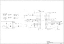
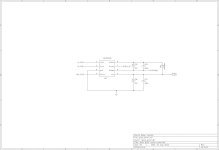
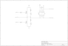
These are the schematics of the controller:
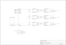
sine_controller.jpg
sine_controller-brainbox.jpg
View attachment 5
sine_controller-gate_driver_B.jpg
sine_controller-output_stage_B.jpg

Just some comments about the DCDC converter (the part that generates the 17V and 5V)
The 12F617 has a comparator with on one input a 0.6V reference source and the other input
is alternated between the 17V and 5V feedback signal. When the feedback signal is below
0.6V the 12F turns on the power transistor (via the ncp5181 driver) for 10 u-sec. After a pulse
a certain wait time (dead_time) is observed to prevent astronomical rise of inductor current
on startup. The 10 u-sec is timed by the CCP module for the 5V supply, the 17V uses TMR2
for timing and the pulse is switched off in the interrupt routine.
On startup the 12F waits around 0.5 sec to allow the capacitors around the gate driver to charge fully,
the first 10-usec pulse has to 'hit the money' so it needs a stable 17V from the zener diode pre-charge
before it can produce the first pulse. After startup has completed and the wait-time after each
pulse has been reduced to its minimum the 12F makes the 'power_ready' signal 'high' to turn
on the main controller IC.

The code on the 12F617 (can be used in MPLAB X):
View attachment dcdc_converter.X.zip

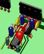
At the moment I'm busy with the gate driver and output stage for 1 motor phase, this is how far I got:
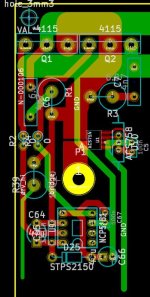
pcb_2d.jpg pcb_3d.jpg
 
You have quite a few top side solder connections. Utilizing via holes and doing all the soldering on the bottom gives a better and more robust pcb. Trust me, I went against my teachers reccomendations on this - and I paid the price by fault checking two sides of the board, not fun.

If you do, however, want some soldering top side (not that I reccomend it) - at least let it be components like resistors. All capacitors should have both solder lands on bottom, as they can't be mounted flush with the pcb with top side soldering.

Edit: I presume, ofc - that you do not have access to through hole plating. If you do, disregard this :)
 
Cool I can't wait to see how this all comes out.
 
Lay it out for TO-247 package mosfets. They are much more robust and avilable devices can handle a lot more current. You can always finagle TO-220 leads into the TO247 holes.
 
texaspyro said:
Lay it out for TO-247 package mosfets. They are much more robust and avilable devices can handle a lot more current. You can always finagle TO-220 leads into the TO247 holes.

They are TO 247's.... I typed 4115 in the schematic as that is the transistor the snubbers are
dimensioned for. But the intention is to use 4568's
 
I'd use SMD for most components. The vertically mounted resistors and caps are simply ugly and completely unpractical.

The RS232 converter looks also odd to me. I'd either leave the serial console at TTL levels as most other controllers have or use MAX232 device or perhaps even USBSERIAL converter.

Just my 0.02 CZK
 
many components especially in the power stage have very high peak currents going through them. The big blue
resistors are typically 2W and can have up to 20A peaks going through. Can SMD handle that ? Plus I can't solder
SMD's 'cause I have a 1960's Weller... The SOIC current sensors for low power controllers are the limit of what
I can handle.
The RS232 works fine with USD->RS232 cables with the 9-pin output and with a laptop having the same 9-pin connector.
USBSERIAL devices are typically SMD only. I don't see the point of a MAX232.

It's been really cold weather here :( , so lots of progress

 
Lebowski said:
many components especially in the power stage have very high peak currents going through them. The big blue
resistors are typically 2W and can have up to 20A peaks going through. Can SMD handle that ?

2W is not problem for SMD.

Plus I can't solder SMD's 'cause I have a 1960's Weller...

Come on, you can solder SMD with virtually any type of micro solder iron with a regulated power. It's actualy much easier and cleaner than through hole and once you start you would never come back. ;)
SMD is fun and the components are cheaper.

The RS232 works fine with USD->RS232 cables with the 9-pin output and with a laptop having the same 9-pin connector.
USBSERIAL devices are typically SMD only. I don't see the point of a MAX232.

I have no doubts that it works. It is just a bit uncommon to use discrete circuit for level RS232 shifting. In addition true RS232 is obsolete nowdays on computers and most people including me use USB interfaces to serial TTL outputs without the RS232 in between.
 
ctirad said:
The RS232 works fine with USD->RS232 cables with the 9-pin output and with a laptop having the same 9-pin connector.
USBSERIAL devices are typically SMD only. I don't see the point of a MAX232.

I have no doubts that it works. It is just a bit uncommon to use discrete circuit for level RS232 shifting. In addition true RS232 is obsolete nowdays on computers and most people including me use USB interfaces to serial TTL outputs without the RS232 in between.
I have a board with a max 232 on it and so far I can not get it to work smoothly.
 
Are you using the same snubbing as previously? Most likely the lower stray inductances in this pcb vs your protoboard setup will allow you to either switch faster or make the snubbing weaker :)
 
Teh Stork said:
Are you using the same snubbing as previously? Most likely the lower stray inductances in this pcb vs your protoboard setup will allow you to either switch faster or make the snubbing weaker :)
Me? I am talking about how the computer comunicates with the dspic30f chip even before I try to run a motor.
 
Teh Stork said:
Are you using the same snubbing as previously? Most likely the lower stray inductances in this pcb vs your protoboard setup will allow you to either switch faster or make the snubbing weaker :)

The snubber components (R and C) are dependent on the transistor (the C) and the board inductance (the R).
So, I can only determine the values when I have to board in hand, the values will be different from before (except
the C when I use 4115's).
As far as switching speed and snubbers go, there is somewhat of a relationship as the power dissipated in the
snubber R is

P_snub_r = f_pwm * C_snub * V_bat^2

This is why I made enough room for 5x15mm resistors, in case 3 W power resistors are used...
 
Lebowski said:
Teh Stork said:
Are you using the same snubbing as previously? Most likely the lower stray inductances in this pcb vs your protoboard setup will allow you to either switch faster or make the snubbing weaker :)

The snubber components (R and C) are dependent on the transistor (the C) and the board inductance (the R).
So, I can only determine the values when I have to board in hand, the values will be different from before (except
the C when I use 4115's).
As far as switching speed and snubbers go, there is somewhat of a relationship as the power dissipated in the
snubber R is

P_snub_r = f_pwm * C_snub * V_bat^2

This is why I made enough room for 5x15mm resistors, in case 3 W power resistors are used...

Yeah, I've been looking into snubbing - but I've not had the need for it with my PQFN fets. But my to220's could probably benefit from this. The major disadvantage with the PQFN is cooling :x

Board inductance can pretty accurately be predicted by 0,01uH per cm, as a rule of thumb :) I don't know about kiCad, but my cad package has this feature built in - you can view trace lengths and from this easily extract variables ;P
 
Impressive! My preference is for IRFP4468 in the TO-247 package - though I have absolutely no complaints towards your goals; it's going to be a lil' beasty regardless.

Not bothered about the SMDs either; pain in the rump to solder. Save it for when you go into production :)
Good on you, KF
 
4468 has amazingly low RDS, might be an option for very small yet very powerfull controllers (limited to 100v of course).
 
gensem said:
4468 has amazingly low RDS, might be an option for very small yet very powerful controllers (limited to 100v of course).
Should actually be limited lower like 20s (84v) fully charged. IR is really good about under rating their fets hence why we can get away with 100v on a 4110 but at the end of the day controller failures will go drop drastically staying below the max voltage limit. It you want 100v or more the 4568 or 4668 fets are much better. Once you run the numbers you can make very close to the same power with any of the three fet choices! Lebowski chose a great one as far as I'm concerned the 4468 is just frustrating to want 110-130 volts on a motor like colossus and be stuck with 84v max.
 
The PCB or controller IC don't determine which FET's you should use, you can solder in 4468's or 4568's dependent
on your supply voltage. Of course snubber values and gate resistors depend on the FETs you chose but the PCB and
controller IC stay the same..
 
The 4468 is a great FET, but IR is a bit behind the curve on thermal packaging for bonding the die to the tab.

This IXYS part is capable of about 20% higher continous current because of it's 0.09Rth die-case vs the 4468's 0.29Rth die-case. Both have nearly identical silicon specs, just more robust bond wires and die to tab bonding from IXYS. It would add about $4 per part for this additional ~20% current, so it might not be worth it for most folks. For someone looking to push the absolute limits of technology, it's currently the best 100v FET I've found in a conventional package size.


IXFX420N10T

http://search.digikey.com/scripts/DkSearch/dksus.dll?vendor=0&keywords=IXFX420N10T


Another really cool package is the newly released 100v offering in the DE475 package. It's built like an SMD part with a ton of legs, but rather than all the fail-boat parts that try to heatsink to the PCB traces (the reason all RC controllers fail), this guy has his die bonded to an excellent thermal path on the back, and as a bonus, it comes all ready electrically insulated. :) You could make an RC sized controller with 6 of the little buggers, just a common rail for positive and negative going down the sides, and the source and drain overlapping in the middle with the phase lead soldered in the overlap area, and then clamp a heatsink to it and actually get meaningful heat transfer.

MMIX1F420N10T
 
liveforphysics said:
Another really cool package is the newly released 100v offering in the DE475 package. It's built like an SMD part with a ton of legs, but rather than all the fail-boat parts that try to heatsink to the PCB traces (the reason all RC controllers fail), this guy has his die bonded to an excellent thermal path on the back, and as a bonus, it comes all ready electrically insulated. :) You could make an RC sized controller with 6 of the little buggers, just a common rail for positive and negative going down the sides, and the source and drain overlapping in the middle with the phase lead soldered in the overlap area, and then clamp a heatsink to it and actually get meaningful heat transfer.

MMIX1F420N10T

Just what I was looking for! :eek: From other sources it seems like the package inductance is under 2nH, making it more than the PQFN - but considerably less than the leaded mates. What makes this really stand out is the thermal path from the fet - I've got to get me some of these :D Can't find any source selling them, so I'll try to get some samples..
 
Yeah,it seems the PQFN package is unfortunately useless for power electronics. Put the worlds best silicon in there, it's still going to make some heat, and on the PQFN package it has no feasible path out of the device, so it's just a matter of time before it fails.

Similar to the IR direct FET package's humorous datasheets. It says some great spec's like 300amp silicon and package limit, then you keep reading, and it says when bonded to a 4oz PCB with 4in^2 of board area with no other heat producing components, it supports 11amps continuously... lol
 
Teh Stork said:
Just what I was looking for! :eek: From other sources it seems like the package inductance is under 2nH, making it more than the PQFN - but considerably less than the leaded mates. What makes this really stand out is the thermal path from the fet - I've got to get me some of these :D Can't find any source selling them, so I'll try to get some samples..

you could try these guys: http://elcodis.com/parts/5894640/MMIX1F420N10T.html

if you can get some, i would be interested too!. (depending on the price ofcourse)


i have been searching for a better fet driver than the mcp5181 i have been using.

so far i have found these two:
http://www.irf.com/product-info/datasheets/data/irs21867spbf.pdf

http://www.ti.com/lit/ds/symlink/ucc27211.pdf

what do you guys think!
 
liveforphysics said:
Yeah,it seems the PQFN package is unfortunately useless for power electronics. Put the worlds best silicon in there, it's still going to make some heat, and on the PQFN package it has no feasible path out of the device, so it's just a matter of time before it fails.

Similar to the IR direct FET package's humorous datasheets. It says some great spec's like 300amp silicon and package limit, then you keep reading, and it says when bonded to a 4oz PCB with 4in^2 of board area with no other heat producing components, it supports 11amps continuously... lol

I've pushed the dualcool fets as far as I think feasible. They are cooled through solder filled vias, trough heatsink on nearby copper on pcb, through top and on the bottom - still the thermal impedance is crap. About 8-10 K/W total for junction to ambient. Also soldering them is a pain in the ass, producing them would need extencive QC.

The fets do handle peaks well tho, so for your 1kW ebike PQFN fets could probably do ok. Either way, looking forward to testing the Ixys fets :)

Nieles: I use TI's TrueDrive series. They parallell a BJT with a mosfet to keep the 0V "hold down" capabillity of the mosfet and the "current driving" abillity of the BJT on the miller plateau.
 
hte ucc27211 part looks nice, due to the internal bootstrap diode however it's limited to a battery voltage of around 100 V.
A feature I really like is that the midpoint inbetween the two FET's, where the load is connected, is allowed to go negative.
 
Back
Top