[DEAD PROJECT] OSBMS - A scalable, low cost, and full featured BMS

Teslafly

10 mW
Joined
Jun 18, 2013
Messages
31
Location
Platteville or Wausau Wisconsin
For the last month or so (and just thinking about it long before that) I have been developing a battery management system based off the ATA6870N-PLPW (http://www.mouser.com/Search/Produc...virtualkey55660000virtualkey556-ATA6870N-PLPW) and an embedded teensy 3.1 microcontroller. This discussion started over on this thread http://endless-sphere.com/forums/viewtopic.php?f=7&t=62995 and has progressed enough that it deserves it's own space.

I have since christened this project OSBMS for "open source Battery Management System".
Because that name sucks though, I am welcoming suggestions for name changes. (Engineers suck at creating imaginative names - I do at least)

My main motivator for this project so far was designing this to be the first module in a complete ev electronics system designed with flexibility, ease of use, and reliability in mind. (and also bringing costs down) Another motivator and guiding factor was to increase the safety of custom vehicles. This board is made to manage anything from a hobbyking battery to <100ah battery banks and be cost effective/reliable while doing it. There should be almost no excuse not to run a bms with this around. (I hope) :pancake:

Goals of project
  • Open source - it seems that almost all gms systems on the market are closed down these days. we want to be able to add whatever features we please as the EV world gets ever more integrated and complex
  • Low cost - The BMS IC was selected to be as low cost as possible with a daisy chain approach used to further attempt to reduce costs through high manufacturing volume. Goal of $2 per cell can be reached. Master board may bump that up for smaller systems.
  • Reliable - Even though a goal is to keep costs low, reliability should not be unnecessarily decreased for small cost improvements
  • Safe - in going with reliable, I don't want this thing to start any fires or cause any damage. I want it to prevent any possible catastrophes associated with using such a power dense energy source.
  • Easy to use - Board is programmed in the commonly known Arduino, but may use an rtos like chibios to facilitate low power-modes and can/usb tasks. Integration with a larger system could possibly be done with ladder logic programming.
  • Multi chemistry - Can monitor and balance almost anything with "lithium" in the name. (lipo, lifepo4, etc. Possibly even super-capacitor banks!)


Progress
  • - A github project has been published and is where I will post most finite progress, but major milestones and discussion will mostly happen here. Link to project: https://github.com/Teslafly/OpenBMS
  • - As of right now I have the slave board with the ATA6870N-PLPW finished and ready to send out to the fab house

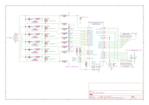
    The schematic:

    A pic of the 3d view on this board
    file.php


    and the schematic
    file.php

    (link to a higher rez (.svg) versionhttps://raw.githubusercontent.com/Teslafly/OpenBMS/master/Docs/Open source BMS.svg as ES doesn't allow .svg files despite their scalability.)

    I will be sending out orders for 5-10 boards worth of parts in the coming week or two. If anyone has a teensy3.1 / arduino and wants to help develop, I am willing to send out assembled dev boards for $20 a piece + shipping (probably $2-5 using USPS). Actual price will drop to ~$12 once in production of 100+ boards.
    file.php


    I am not planning of assembling any master boards at this time until rudimentary cell monitoring / balancing is working as all we need until then is spi connectivity to a ribbon cable. Though if enough dev people say otherwise once I finish the design I will consider putting some masters together.
  • - The master board with the integrated teensy is almost done and will be committed to github soon. (features below) Either a bootloader will have to be made / gotten for the integrated teensy 3.1, or preprogrammed MINI54TAN bootloader chips will need to be bought from PJRC. (As of right now I am going with the bootloader chip)


Keeping the project goals in mind, here are the specs for the master major system boards. (If there is something you think is too much, or is badly needed, these specs are still quite flexible)

Master Board Features
  • Teensy 3.1 Micro-controller (MK20DX256VLH7) (Possibility for alternative simpler/cheaper master with atmega328 where advanced features aren't needed? comments?)
  • USB programmable with a possibility of usb otg for android devices / dashboards.
  • 2-3 current sensor inputs. one for charging, one for the motor. (one for AUX?)
  • Input voltage sensing
  • Several (2-4) mosfet controlled outputs with the option for a current sensor on at least one (or one sensor for all of them?). NPN switching (or PNP if people want?) This can be used to control a contactor, precharge circuit, fan, etc.
  • Onboard switching regulator to bring pack voltage down to 5-12v when system is on. (Microcontroller will run off ATA6870N supply when unit is off. This should result in a current draw <100ua)
  • Connectors for an LCD Display and all extra pins broken out for auxiliary I/O.
  • SD card slot for datalogging (and configuration via txt file?)
  • Opto isolators for controlling charger or communicating to voltage shifted masters.
  • Onboard CAN transceiver for data connection to other modules. (This will probably take me a while if no one else does it. CAN has a very steep learning curve, but I do want to get into it eventually as it is used in almost every high reliability industry)
  • Analog and pwm throttle input & output. This can map the throttle to different values, change a analog signal to a pwm one, or/and cut/hold back throttle when the pack is almost empty/dead.
  • Onboard buzzer / alarm - If something goes severely wrong, this board will let you know


Slave Board Features
  • Measures 4-6 Li-Ion Cells in Series
  • Stackable Architecture Enables >400V Systems. (Up to 16 6s modules) - Master modules can be isolated and daisy chained as well for even higher voltages. This will be implemented once the system is rock solid and someone comes along that wants it and is willing to test it.
  • 0.25% Maximum Total Measurement Error (12 bit adc) - This will be tested in reality once the first boards are constructed.
  • Extremely low power when asleep. (<100ua)
  • Two Thermistor Inputs - One connected to an On-Board Temperature Sensor and the other one brought out to a header.
  • Cell Balancing:
    • Balancing achieved with 10 ohm power resistors. This means ~1.8 watts power of dissipation per cell. Heatsinking is probably needed at this level for full balancing current.
    • The onboard thermistor will reduce the duty cycle of the resistors in 25% increments (from 25-100%) to keep the board from overheating / melting. If the system overheats it will shut itself down. (This action is fully programmable)
    • Predictive cell balancing? If a cell always needs a certain amount of energy removed while charging the board will preemptively balance the cell. I know of no example of this and will investigate its utility


ToDo:
  • Figure out mounting holes - The slave board is so small there is almost no mounting hole room. with the ability to mount this board to a heatsink with a thermal pads probably needed, I'm thinking half moon cutouts on the top and bottom of the board
  • Programming - no program exists for this yet, and the first thing on the list is to get cell voltage reading working, then the balance resistors and heat management, then the actual computation and proper monitoring of cells that you would need for a working basic bms. Then we take it from there.
  • Finish master board layout
  • Create a cheap master board using atmega328 / atmega32u4?

So with all of that being put out there, what do you think? and what would you like to see in your "dream" BMS?

* edit, changed name form "OSBMS - yet another "open source battery management system"" to "OSBMS - A scalable, low cost, and full featured BMS" beacuse I think it is much more descriptive and what I probably should have gone with in the first place.
 

Attachments

  • Open source BMS lowrez.png
    Open source BMS lowrez.png
    45.5 KB · Views: 10,010
  • bom prototype pricing.png
    bom prototype pricing.png
    40.6 KB · Views: 10,009
Why the 100ohm resistors between Vdd and ground?

In addition to my comments on the previous thread, I would add some ~5.1V zener diodes in parallel across each cell input. They will keep the MBAT inputs below the max in the case of a broken wire, or when you're plugging the battery cable in or disconnecting it. Take a look at the schematic for my board in https://github.com/dmwahl/BQ76PL536A-Arduino-Development-Shield and you'll see what I mean.
 
For $120 ish the mouser / atmel dev kit looks good to try:
ATA6870-DK10.jpg

ATA6870-d10
Has a good pdf http://www.mouser.com/ds/2/36/doc9228-75653.pdf

What do you think of the dev kit with active balancing using the ATMEL ATA6870
ata6870-dk11.jpg

see http://www.atmel.com/tools/ATA6870-DK11.aspx
pdf : http://www.atmel.com/Images/Atmel-9...70-and-Atmel-ATmega32HVB_Application-Note.pdf

But the inductor pwm is implemented from the host uCro over spi and the suggested max pwm rate o3kHz makes the inductors large.

The dev-board_ata6870-dk shown with extra host board under 18s demo board is not included as far as i can tell.
dev-board_ata6870-dk.jpg

and pdf http://www.atmel.com/Images/doc9171.pdf

General info on the chip series pdf http://www.atmel.com/images/doc9019.pdf

You'd think i'm a rep for atmel ... no rep for any one just adding all links here to save time for others.

I like the longer pads the have have on the dev board for the qfn-48.

The bridging connector footprint looks like one membrane. is this cost effective?

Do the unused bridge ports need to be terminated?

THe pdf doc on broken sense wire.

But if the cell inter connect breaks higher voltages will be between the break. Say for a 24s pack 100V.
How does the circuit handle this?
 
Why the 100ohm resistors between Vdd and ground?
If you look at the ATA6870N reference schematic It has them as well and specifies their value in the datasheet. I believe that the ATA6870N chip has tvs/zener diode protection built in - Hence the 1k resistors on the voltage sense inputs and 10 ohm resistors on the power pins. I will test to see if the board will self destruct under adverse conditions but I believe it will be just fine. If it does get damaged I will add them in a later revision.

Thanks for the links 7 circle. Many of them will sure be useful later on.
As for responses to your questions

For $120 ish the mouser / atmel dev kit looks good to try:
I can build 2 boards for ~$40 and test my design at the same time. I also want to use a different micro-controller then they have and that will be more troublesome with the dev board.

What do you think of the dev kit with active balancing using the ATMEL ATA6870
I think it is only marginally better with much higher (2-3x) higher cost. If energy was at a premium and cost was no objective I may have gone that route,(Like if I was building a satellite) but discharge resistors waste relatively little energy and are much cheaper, which is one of the major design considerations of these boards. It's kinda funny though, it seems like they are just bit banging the balance outputs on and off as fast as they can to achieve this active balancing. 3khz is the spec because it's the fastest they can bit bang it on and off. This is a bit of a problem because as more ic's are added the fastest they can bit bang it drops and inductors get pretty large.

I like the longer pads the have have on the dev board for the qfn-48.
I may go to this if it proves to be a problem. As of now I am just being lazy and using the built in kicad QFN48 footprint.
I will be assembling these boards using a home made solder paste stencil and then a hot air rework station to reflow the board as my toaster oven is approximately 400 miles away at the moment.

As for testing later on I have 10 hobbyking 4s 5000mah hardcases to use in any combination I feel like testing. 4s 50ah? I can do that. 40s 5ah? I can test that as well. I am going to start at 12s 15ah for now though.

The bridging connector footprint looks like one membrane. is this cost effective?
I'm... not sure what you mean here. Could you be a little bit more clear? If you are concerned about the connector cost itself the bom is posted on the github repo in the docs folder. The connectors are $0.55 each in quantities of 25. This is slightly more expensive that I would like, but I opted for a smaller connector with locking ability for better reliability and space management. link: http://www.digikey.com/scripts/DkSearch/dksus.dll?Detail&itemSeq=158115033&uq=635482884596040971 If you want though, you could stick them all on one board without connectors and have the system be less scalable for more popular cell counts. The github repo is ripe for the forking. :D

Do the unused bridge ports need to be terminated?
Yes, the upper board's upper datepins need to be shorted to vcc on that board. This is all specified in the datasheet.

But if the cell inter connect breaks higher voltages will be between the break. Say for a 24s pack 100V.
How does the circuit handle this?

If a single sense wire breaks the ic will be able to detect it and throw an error. It shouldn't damage the ic. If the balance connector to an entire ic is disconnected with the ic's above and below it are still connected. It's intrinsic power draw and power connections between chips via the data bus should protect it. With this board being hot pluggable this is a valid concern. Once the code is working failure modes will be investigated and additional protections will be added if needed. If you want, you can put together a list of tests for failure modes to investigate when the test boards are complete.
 
How's it going? I'm mentoring some students on open source EV stuff and this looks perfect. I've got a lot of reading to catch up on it but I wanted to know if this is still moving and if you would like some help. I have an ebike with Headways that I can use for development.

Thanks,
Gary
 
Development wise this project has slowed but not stopped as of late. School has been a bit more work intensive and I haven't had that much time to work on this until this weekend rolled around. I have started writing code and believe I have most of the rudimentary communication pinned down. This version does not use a rtos, but most of it's functionality is implemented in subclasses so it shouldn't be too hard to transition.

for hardware, I am about a week away from ordering the parts from mouser/digikey, and I will be ordering boards near the same time. my plan right now is to get the boards fabbed at seeedstudio, with 10 5x5cm balancing boards (ordering enough parts for 5 boards in regards to the ata68 ic and connectors, but passives will be bought to fill 10+) and 10 master (atmega328) containing boards with some power semiconductors and communication bits that I haven't published yet. (But plan to do tomorrow. Watch my github! https://github.com/Teslafly/OpenBMS)
I am going with atmega328 master boards because they should be vehicle ready, just no advanced functionality and no can bus communication. For arm (teensy 3.1) development I will just be making a protoboard setup as a complete fabbed board is a little pricey for me as of right now.

If you want to help out on this project, please let me know via pm. Preferably before I order parts next weekend as more prototypes help costs go down. I am willing to sell the balance and slave boards at parts cost (approximately $20 for the balance board, not sure about the master board yet. under $30) to anyone who wants to help develop it. My goals right now are to get balancing and temperature management working, with contactor/psu control and datalogging/etc coming after that. I theoretically have voltage measurement working in my code right now, but I have no boards to test on at this point.

- Marshall
 
UPDATES!

REV 1 is ready for prototype manufacture.
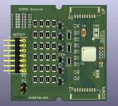
The Rev 1 Balancer board has had it's silkscreen cleaned up, mounting "holes" added, and BOM completed. All parts are selected and ready to be ordered.
The final estimate for parts cost is ~$18, not including solder paste and other manufacturing stuff.

file.php

Balancer Front

file.php

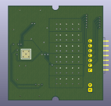
Balancer back

Along with all of this I have updated the docs folder on github: https://github.com/Teslafly/OpenBMS/tree/master/Docs
I have uploaded pdf's of all schematics and higher resolution renders of each board than are available here.
I have also completed the bill of materials for both boards and posted them there.


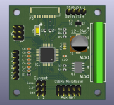
The Micromaster board has been released in it's complete glory. It contains an atmega328 ic for prototyping (everything should remain portable to ARM during this time)
and contains the following features

* Atmega328 main processor @ 3.3v - 8mhz. Programmable through arduino with usb -> serial adapter (Program it just like an Arduino pro mini)
* Runs completely off power output from slave board/s. This is convenient but allows no SD card or indicator leds as the ATA6870N can only supply 20ma
* 2 dedicated current sensor inputs. Useful for sensors like the ACS759
* 2 auxiliary 12-24v 5A NPN mosfets. (current is untested!) The voltage on this auxiliary rail is also monitored via a voltage divider. This is for controlling contactors, fans, etc
* 1 connector for a precharge circuit. Outputs for 1 small relay and a protected adc input for a controller voltage monitoring circuit.
* All other I/O pins are brought out to a 10 pin header along with 3.3v and GND.

The Micromaster should cost around $12 to make in parts costs, so it is much better than I initially predicted.

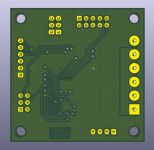
file.php

MicroMaster front

file.php

Micromaster back (I ended up carving out more of the back ground-plane on this board than I would have liked, but it was necessary to get everything where it needed to go.

So that's the complete <icroMaster board. You would almost certainly use a bunch of the auxiliary pins if it were to be used on any EV, but basic, catch all functionality is going to be ok with it.

As I move along in this project and get to later revisions, this will probably become more inclusive functionality wise, but I'm not sure what I would add on top of this. If you have time to look at that is there, would you suggest features that you would like on a simple BMS system that aren't already specified under the MajorMaster?

Moving on,
The test program is looking good. I believe I have it to the point where I could plug it in and start reading cell voltages off of a 16 cell stack.
If any bug-fixes are needed, they should be small and somewhere in the initialization of the chip.

The next steps for programming is to get the Checksum working(LFSR based), as well as the balance resistors working. The balance resistors are just 6 bits in an otherwise empty register, so I may just create a routine to toggle them on and off for testing while I figure out the most efficient way to achieve balancing.

In that realm, does anyone know what the most efficient balancing method would be? I could always just shut off the charger when one cell reaches max voltage and discharge all cells to the lowest cell, but that seems like an extreme waste of time.(Along with an opportunity for too much thermal buildup.) Is there any way to predict which cells will need to be balanced while charging and preemptively start to balance them? This would be the sort of balancing I would like to implement in this system as it saves time and spreads thermal dissipation out over a much longer period. (I could probably puzzle this out with experimentation, but I don't want to if I don't have to.)

Well, there's Rev1. Please let me know what you think and If I made and critical / obvious errors.
I will be sending this out to be fabbed as soon as I hear back from some people interested in helping develop this system.
 

Attachments

  • rsz_osbms_balancer_rev1_final.png
    rsz_osbms_balancer_rev1_final.png
    94.3 KB · Views: 20,722
  • rsz_1rsz_osbms_micromaster_rev1_final.png
    rsz_1rsz_osbms_micromaster_rev1_final.png
    53.3 KB · Views: 20,723
  • rsz_osbms_balancer_rev1_final_back.png
    rsz_osbms_balancer_rev1_final_back.png
    108.9 KB · Views: 20,722
  • rsz_osbms_micromaster_rev1_final_back.png
    rsz_osbms_micromaster_rev1_final_back.png
    113.2 KB · Views: 20,722
Teslafly said:
.. In that realm, does anyone know what the most efficient balancing method would be? I could always just shut off the charger when one cell reaches max voltage and discharge all cells to the lowest cell, but that seems like an extreme waste of time.(Along with an opportunity for too much thermal buildup.) Is there any way to predict which cells will need to be balanced while charging and preemptively start to balance them? This would be the sort of balancing I would like to implement in this system as it saves time and spreads thermal dissipation out over a much longer period. (I could probably puzzle this out with experimentation, but I don't want to if I don't have to.)...
stopping the charger as one cell hits LVC is a MUST for a BMS. i guess this is a given fact. but having to bleed this cell down to the rest of the lower cells really is a waste of time. if you can't reroute the current from the leading cell to the following/lower cells, then you would need to start bleeding during charge already. i guess with the programmable controller you can set this "start to bleed during charge" voltage to a user defined value, as all packs are a bit different. eg rc-lico has very little capacity between 4.1 and 4.2v. so once a cell reaches 4.1 and is charged with 1C it takes very little time for this cell to go to 4.2v while the rest may still be below 4.1v. so it would be a good idea to start bleeding this cell at some voltage just below 4.1v. of course this would prevent the whole pack to be fully charged - well not prevent, but it would take much longer because the more cells reach 4.1v, the more cells will be torn down. so there must be some algorithm to raise this "start to bleed voltage" not be be lower than the lowest actual cell, in fact it has to be a bit higher even.
i hope this helps ;)
 
Teslafly said:
.. In that realm, does anyone know what the most efficient balancing method would be? I could always just shut off the charger when one cell reaches max voltage and discharge all cells to the lowest cell, but that seems like an extreme waste of time.(Along with an opportunity for too much thermal buildup.) Is there any way to predict which cells will need to be balanced while charging and preemptively start to balance them? This would be the sort of balancing I would like to implement in this system as it saves time and spreads thermal dissipation out over a much longer period. (I could probably puzzle this out with experimentation, but I don't want to if I don't have to.)...
Turn on the balance resistors once the SOC starts to be a function of voltage but before you get to max cell voltage. For LiFePO4 this would be around 3.5-3.55V. When any cell gets to the max, then cut the charger. It will take some time on the first balance, but after that it takes much less time.

Most "dumb" or analog BMSs combine the balance and HVC functions into one, when ideally they should be separate. HVC should cut off the charger to prevent overcharge, whereas the balance function can operate before hitting the HVC point. This is why it's easy on analog BMSs to overpower the balance resistors and overcharge a cell if the pack is too far out of balance.
 
By the way, very similar design:
http://ev-power.com.au/webstore/index.p ... cells.html

... Not really. not really at all.
All BMS systems are going to have a bit of the same design concepts because they accomplish the same function, but the board you linked to really doesn't have anything to do or contribute to this project.
Rather, it is part of the problem it is trying to solve.
As you can see, while it does "manage" 12 cells, it is not capable of balancing them and can only tell you when there is a fault.
second, it has been rendered a "dumb" system. yes you can set the balance voltage, but cell reporting and software configuration is impossible.
Thirdly, customers can't really get custom functionality out of it. It says "proprietary" right in the product description. Something tells me that's going to be quite a headache.
Finally, is quite expensive for what it does. ~$90 to basically tell you is anything is wrong, nothing more. If you set up my published system to do exactly what this board does plus some it would only cost $55 and give you so much more power and flexibility that you'd probably forget that that system exists.

So while thanks for the link, I don't think there is much to be learned from that product.


Turn on the balance resistors once the SOC starts to be a function of voltage but before you get to max cell voltage. For LiFePO4 this would be around 3.5-3.55V. When any cell gets to the max, then cut the charger. It will take some time on the first balance, but after that it takes much less time.

Ok, I think I get what you are saying. the voltage vs SOC curve starts to flatten out towards the end of the charge so you can just inference the SOC of the cells from the voltage and start balancing the high ones then. I think I may have an idea on how to implement this, thanks.


And yes, HVC and LVC will still work the same as these are safety critical "NO CROSSING" lines. I'm just trying to figure out how to make balancing more time efficient and that won't effect the safety cutoffs. (In fact it may improve their triggering)
 
Just so I understand correctly, the standard "48v" 13S system would require 1x master and 2x slaves, with the last slave being used for the final 1S unit ?

-=dave
 
Just so I understand correctly, the standard "48v" 13S system would require 1x master and 2x slaves, with the last slave being used for the final 1S unit ?

Do you mean 12S system? I am unaware of 13S being a standard, but am aware of 12S, 16S, 20S and 24S being pretty common.
Each balance board can handle 4-6 cells, so for 13 cells you would need 3 boards, and
because they have a minimum of 4 cells par balancer you would need 5 cells the first board, 4 cells for the second, and 4 cells for the third.
13S is a really suboptimal setup for this system, but not impossible.


Also, with the release of Rev1, I have been looking at licenses.
What are peoples thoughts on the GPL 3.0 license for this project? http://choosealicense.com/licenses/gpl-3.0/
 
Huh, well I guess that this system wouldn't be the best for them unless they wanted to spend the extra $ for a 6s board that effectively manages 1 cell.
You may be better off knocking off a cell or using a cheap Chinese "BMS" for those lower power setups.
Blocks of 6s are the best, but if you can get at least 4s across every board, it will work.

Parts have been ordered for 10 Balancers and 5 microMasters. I'll update when I get the parts and assemble the first board to test the firmware.
 
Teslafly said:
In that realm, does anyone know what the most efficient balancing method would be? Is there any way to predict which cells will need to be balanced while charging and preemptively start to balance them?

The standard for MP-controlled LiPo hobby chargers is to:

Perform test discharge of main pack at a fixed (calibrated) discharge; while doing so calculate individual equivalent Internal Resistance of each cell: R(int) = V(cell)/I(dischg)

Use this R(int) for each cell to determine safe balance over-charge (usually limited to 50mV in practice but 0mV in ultra-conservative design. This could be configurable)

If V(cell1), V(cell2), ... V(cell n) > V(min) && < V(max) - 0.1V begin I(max)charge
If V(cell1), V(cell2), ... V(cell n) < V(min) begin I(restore) charge [this is typically 1/20 C, to slowly restore an over-discharged cell as safely as possible. A timer should be configured so that if restoration fails, I(restore) stops with ERR
If V(cell1), V(cell2), ... V(cell n) >= V(max) - 0.1V begin V(max) charge [with balancing]
Monitoring V(cell 1...n) if V(cell n) >= (V(target) - 0.1V) && V(cell n) - V(cell min) >= 0.1V, engage I(bleed cell n)
Stop charge when V(cell 1..n) delta < balance target [this should be configurable but is typically 0.05V (fast charge) - 0.01V(slow charge)]

Some typical values:
V(cell min) = 3.0V [2.5V for older chemistries but really, there is such little power between 2.5 and 3.0 that using 3.0V is the safer option]
V(cell max) = 4.2V for max range, 4.1V for reasonable cell life (this should probably be the standard), and 4.05 for extended cell life. Should be user-configurable like all other values of course
I(restore) = 1/20C or lower

Without the ability to perform a discharge and such (no charger control) I think the balance monitoring is relatively unaffected, since there are no additional voltage monitor rails for the balance taps.

I realize this is not a charge/balance board, but figured I'd show you what I know and you can figure out what capabilities you've built into your board (as I've not completely reviewed the design yet).

-=dave
 
caveat: this is for 4.2V LiPo chemistry. I'm unsure of the LiFe voltages but I would imagine the same delta values would work, while the V(target) would just be lower.

-=dave
 
i've just started taking a closer look at your excellent work Teslafly!

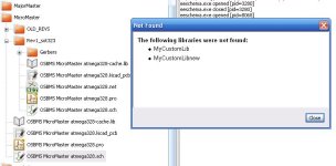
i cloned your github repo and opened it in kicad and got this error:

openbms-kicad-error.jpg


i'm brand-new at kicad, so please tell me what can i do to fix this.

Thanks,
ted
 
I know one of the issues of building a fully adaptable BMS (one usable from a single cell up while drawing proper voltage) to produce 5v from even a single cell.

http://www.adafruit.com/product/1903

I located this on AdaFruit and while 9.95 is a bit much per unit, the PCB is based upon the TI Chipset:
http://www.ti.com/product/tps61090

I figure this should make generating 5v from an emergency battery or a 1-2S pack a piece of cake... This will allow adaptation to work from 1S to however many you wish to monitor.

Hope this is useful info!

-Mike
 
Well, A lot has happened since my last update. I've been working on the BMS almost the entire weekend and have made lots of progress.
(aka, boards assembled, code tested with balance resistors and voltage measurements -intermittently?- working)
I'll post the actual update tomorrow or tuesday (hint, it's long) and for now just answer some posts that have popped up on the thread.


tungsten2k said:
Perform test discharge of main pack at a fixed (calibrated) discharge; while doing so calculate individual equivalent Internal Resistance of each cell: R(int) = V(cell)/I(dischg)

Use this R(int) for each cell to determine safe balance over-charge (usually limited to 50mV in practice but 0mV in ultra-conservative design. This could be configurable)

Hmm, acquiring that data may be possible, but will probably be more tricky as you may not have direct control of the charger. You should have an amperage reading though.
I'll have to do a couple charges and discharges on various batteries with this system logging voltages to see if a modification of this will work. especially for different chemistries... (I don't see why it wouldn't)
And yes, everything should be configurable. I try really hard not to hard code things in as it's a pain to adjust things later.


trl said:
i've just started taking a closer look at your excellent work Teslafly!

i cloned your github repo and opened it in kicad and got this error:

Yeah, that is to be expected. My fault really. kicad's library management is crap and it doesn't store a separate cache of symbols with the project. (which I forgot about.) I wasn't careful and didn't consolidate parts / symbols into the library included with the other github stuff. Is anything obviously missing? You should be able to open the project anyways and see if those missing libraries broke anything.


izeman said:
how is the project proceeding? I would like to test that bms ...

Does this make you more or less hungry for the full writeup?
https://www.flickr.com/photos/76027390@N05/sets/72157649986107399/


I know one of the issues of building a fully adaptable BMS (one usable from a single cell up while drawing proper voltage) to produce 5v from even a single cell.

even if I was running stuff off a single cell, I would choose a 3.3v microcontroller so I could just use a LDO or such. As it stands the ATA6870n ic's have built in voltage regulators that draw current evenly from across the pack, so powering the microcontroller and other low power peripherals won't be a problem.
 
There are no provisions at the moment for full current battery passthrough. There are two npn power mosfet outputs that could be used to drive a contactor or your own high current mosfet bank though.
I made this decision because I figured it was much easier, cheaper, and scalable to use simple low current i/o to control chargers, motor controllers, and other devices connected to the battery then an integrated high current switch.

The update stuff is chugging along. The build section is finished, and the code / suggested features section is nearing completion as I work out the bugs of this preliminary code. (plus I just found out that I have to provide a 500Khz clock to the ic instead of the other way around. This was apparently a footnote I missed in the datasheet. So make that 3 bodge wires for this prototype.) That said, I am at 100% reliability for data reads / writes.

If I can't finish the code section tomorrow I'll just post the build section separately and the code section sometime this weekend. I'm late as it is.
 
so you would not let the dis/charge current run through your circuit, but have an external switch triggered when you hit HVC or LVC? good idea. why not?! :)
i already have an inrush limiter switch that can be turned on/off by supplying a voltage with minimal current to some power mosfets.
or you could just feed a relay that turns on/off the controller and charger directly. correct?
unfortunately i was too late to become one of the testers. but i definitely would like to get into the first production queue please :)
 
Back
Top