DIY Programmable BMS (now using ATtiny/Arduino)

powersupply said:
dmwahl, off the bat, I noticed a few things and I just let them out as they are.

Please consider some mounting holes which would not collide with possible sliding rails of eurocard enclosures.
Why would you use the mounting holes if the board is in a eurocard enclosure? It's sized to fit into the card rails. I added the mounting holes because I can't stand anything without them, but they aren't always needed.

Power resistors can get rid of heat WAY much better if you stand them up (in case you have the headroom).
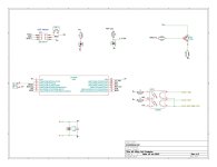
Yes, perhaps, although heat transfer is a complicated beast, I've spent years doing it professionally for military/industrial computer boards and there's no one rule like that that always holds true. A lot of heat transfer out of leaded power resistors is through the leads, but standing them on end makes them more prone to mechanical damage. What you can't see in the render I posted is that the back side has a large copper flood connected to one of the leads.

I would also suggest some staggered connectors for folks like me who have 4s1p (or 5s) packs.

F.I I am using 13s4p made out of 13 4s1p hardcase packs.

I would solder the socket for the first pack into C1..C5 no problem.
But where do I solder the socket for the 3 pins I removed from the next 4s connector?
This is missing from every approach I have seen.
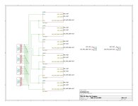
I don't quite follow what you're trying to do here, do you have a picture you can share?

I think you place your stuff way too close to the edges of your layout.
There silkscreen outlines are larger than the actual parts, I've printed the layout on paper to check component clearance and had no issues. Hard to tell from the render though.

Just skip one stage , how many would need a 36s unit?
?

Please keep in mind that I have not really aquainted myself with your design, so if something is off I apologize in advance.
Just posted this as I had the impression that you want to order the PCBs.

How much is the total cost of the BOM for a 13s setting BTW?
I appreciate the feedback. BOM cost for 13S would probably be around $45 from Digikey. Most of the parts can also be found on ebay for less if you don't mind waiting for shipping from china.

One major concern I have with using mictocontrollers is their operative reliability.

None of these BMS units -be it DIY or produced- have any type of safeguarding against most common EMF or similar external disturbances.

Even with watchdogs active we could knock out PICs by just holding one of those nasty Nextel phones close to them while calling the phone.

Based on your experiences, did you ever have a unit go berserk and you had to reset it to work again?
I haven't had any issues with stability. How did you solve the problem of knocking out PICs with a phone? Were they actually damaged?

Thanks again for the comments.
 
peterperkins said:
As someone who has built several BMS over the years based on individual pic devices for each cell I have the following comments.

1) Nice project and you have the sleeping current down to very low levels. All looks and sounds quite familiar :)
Thanks, glad to know I'm not the only one crazy enough to try it.

2) The voltage drop in cell connection leads for remote boards is a significant problem when the bypass load cycles. Unless you have a huge amount of hysteresis/very thick wires then as soon as the load turns on the voltage detected by your chip will be significantly lower and probably turn itself off again.

Also adjacent cells sharing cell wires will also tend to interfere with each other. I strongly suggest bench checking how three modules perform on the bench using say 500mm leads using the ones at the ends fed by say a fixed voltage and the one in the middle fed by a variable voltage so you can tweak it up and down and see how it and the adjacent cell/boards respond. Two wires for each terminal removes the adjacent cell interference issue but not the voltage drop in the wires problem.

I have my slave boards controlled by a master board which commands all the slaves to turn off the loads before any measurements are made by the pics. Once the measurement is made then the slave loads can be turned on according to the voltage for each cell. This negates the voltage drop in the wire and the adjacent cell issues completely. In fact it was the only way I could get reliable operation when the cell wires are fairly thin and over about 300mm.

I use a 1S loop/refresh for routine voltage monitoring when driving.
When grid charging though when the first cell cell starts to balance/bypass you can slow down the bms loop/refresh to say 5s this gives the load maximum time to burn off energy between voltage readings.

My first BMS based on the picaxe chips 08M 12F683 was made of individual boards on each prismatic cell, that never suffered from the voltage drop/adjacent cell issues and has operated uninterrupted for 5 years since the boards were first fitted to the cell. That's a pretty good test.

All the code developed for the various boards etc is in the PD on
http://www.batteryvehiclesociety.org.uk/forums/viewforum.php?f=53
I appreciate the feedback on this. I've been debating with myself about how to deal with the voltage drop issue, and at least on a single cell level it hasn't been a problem. I've monitored the cell voltage independent of the BMS circuit and it still prevents overcharging, but I think you're right and I will need to synchronize measurements. Have you found that you need a settling period after turning off the shunt and before measuring cell voltage? Currently I have the BMS measure cell voltage every second, turn off the shunt before measuring, and sleep for 16ms between turning off the shunt and taking a measurement.

Is the communication between your master/slave boards single directional? Or can you actually get data back from the individual monitors? You can't tell from the rendered pcb, but the Px02 headers on my board are tied to one of the AVR pins to drive a pin change interrupt to sync the boards. Not yet implemented in the firmware though.

3) The cell voltage measurements do not need to be accurate to the n'th degree. +/-25mv is fine.

4) I used oversampling on a 10 bit adc and a standalone 1% 1.235v reference on the first two versions of my BMS. Lately I have used the internal Vref reference on the 12F1822 pic which has proved to be accurate enough and simplifies the board quite a bit.
Did you need to calibrate the PIC internal Vref? I would need to on the AVRs and didn't want to deal with it right now. Some day I will though. I only chose the AVR platform since I was familiar with it, I'd like to experiment with PICs as well since a lot of people seem to like them. TI's MSP430 has also caught my attention.
 
The mounting holes could be used to piggyback some other board(s).
Like a telemetry board or some bluetooth module or other things.

We did exhaustive tests with (heated) resistors in sealed enclosures many years ago with a local university.
Result was clearly that the farther the resistors are from any object (be it PCB), the more heat they were able to radiate.
In high g scenarios we used wire barrels to support the resistor. Helped dissipation, too

The PICs (and other microcontrollers, too, BTW) would only come back to life either by dis/reconnecting them from/to power, or by a hard reset.
No NMI or other interrupt like the mentioned watchdogs could bring them back.
The issue are the bursts of high frequency/energy which is collected by the traces (they act like antennae).
It is recitified by the clamping diodes inside the chips and that results in a huge amount of energy causing havoc.
Either by lifing the VCC to higher levels than allowed or by just going all the way to the CPU and zapping it.
When zapped the uControllers would still work somehow, but what they'd do was unpredictable/unclear.
They would not get destroyed (at least not that we could measure).
The remedy was shielding the whole thing and filtering any wire entering. In really critical enviroments (a 50kV paitning/laquering facillity FI) everything was put into a wholly shielded metal case. The only pins entering (with heavy, 3 stage filtering) directly was the power to the unit. Everything else went optically in/out.
But that would be too extreme here.
I just wondered with all these BMS because everything is totally open, with many wires (antennas) entering to it, and no HF filtering whatsoever. And we have cellphones everywhere....

Thanks, P
 
I have no doubt that I could improve the heat transfer off the power resistors, there's no practical reason to do so though. I've measured the surface temp, and it only gets up to around 60-70C on a breadboard, with a big copper flood underneath it that number will only improve. I'm not running them anywhere near their limits.

I've looked at lots of similar designs, and none that I've seen include anything more than basic filtering on the inputs. If you think that's a bad idea in this application I'd appreciate the feedback. I'm trying to keep things as simple as I possibly can here.
 
Schematic for one of the cell monitors attached. The other 5 cell monitors are identical. As it stands right now, each board contains six cell monitors, four 6S JST-XH connectors to parallel multiple packs, one HVC, and one LVC header. Multiple boards can be used, so not limited to 6S packs.
 

Attachments

  • ATtiny-BMS.jpg
    ATtiny-BMS.jpg
    164.5 KB · Views: 4,397
  • ATtiny-BMS-Cell1.jpg
    ATtiny-BMS-Cell1.jpg
    142.5 KB · Views: 4,397
Yes, a very important question. Processors can crash and leave things in strange and sometimes dangerous states.

Cars use processors and they go to great lengths to handle dangerous conditions.

Airliners use processors and employ multiple redundancy with numerous interlocks and failsafes.

You need to think about all the possible states and conditions and try to deal with them.

I had a very early bread machine that was run by a microprocessor. It baked a lot of fine loaves of bread, until one day the processor crashed in bake mode. The processor was in control of the heating element. I smelled the plastic top melting before I became aware I needed to unplug the monster before something caught fire. The manufacturer quickly added a failsafe that would override the processor if necessary to keep the temperature from soaring out of control.
 
Assuming HVC and LVC will never be active at the same time you can save a resistor by paralleling the Anodes of U203 via one resistor to B+
Make sure you do something with the spare pins on the processor, tie them to ground or whatever.
You don't need the 5.1V zener.
Use a npn transistor for the load control.
Put an led in series with the transistor base resistor so you have a visual indication when the load is on.
Tie the load resistor transistor controlled side to a spare adc input as well, then you can detect if the load is being powered when the led is not lit, perhaps caused by a transistor fail short circuit.
If the chip has a pwm module which outputs on a specific pin use that as the load driver pin then if you want later you can implement proportional balance current control via pwm.

My slaves read the voltage about 250ms after the load is turned off.

My bus can pass info in both directions. I have a separate master and slave bus. Master send commands on cascade slave bus. Slaves respond on parallel master bus. I don't have contention issues as slaves forward messages along the string to each other. So only one can be using the master bus at anyone time.

I didn't calibrate anything other than checking results were acceptable with my DMM on a few sample devices :shock:

My slaves recognise and respond to the following commands.
They are not individually uniquely identified. All run the same code.
But the master knows their position in the cell string.

' Command 01 = Read and Send Cell Voltage on Master Bus
' Command 02 = Turn Off Loads
' Command 03 = Turn On Loads if Reqd by last cell voltage reading
' Command 04 = Increase Load CutIn Voltage by 50mv
' Command 05 = Decrease Load CutIn Voltage by 50mv
' Command 06 = Set Slave Load CutIn Voltage Default
' Command 07 = Turn On Slave Load for 0.5 seconds (Flash Led) Useful for comms testing.
' Command 08 = Report Slave Software Version Number (Useful to ensure all running same version)
' Command 09 = Increase FailLow Cut Off Voltage by 50mv
' Command 10 = Decrease FailLow Cut Off Voltage by 50mv
' Command 11 = Increase FailHigh Cut in Voltage by 50mv
' Command 12 = Decrease FailHigh Cut in Voltage by 50mv
' Command 13 = Set FailHigh/Low Voltages to Default

Issues I found with emi/rfi interference were.

1) The pics are incredibly resistant and I never had any lockup issues.
2) The master bus is sensitive to interference (paralleled via all the slaves) :oops: which is the weakness in my system.
I should have used a current loop or something else rs485 etc.
So my slaves echo recd commands back to the master for checking. You could use much more sophisticated error correction.

Peter
 
The avr pins have the internal pullups enabled, so they are pulled high.
The zeners are for protection when connecting or disconnecting a multi-cell pack. Since not all the connections get made at exactly the same time and current drawn by the micros will vary during startup, the supply voltage to an individual monitor could rise above max. See this post for my explanation why.
Why use an npn instead? I used a pnp so I can take advantage of the internal avr pullups and not need another to ensure the transistor base doesn't float.
I did connect the base pin to a pwm output for exactly the reason you mention. PWM on the atmel chips is extremely easy to implement, I think it took only 2 or 3 additional lines of code compared to non-pwm control.

I've had several questions why I use an external reference when there is an internal one, and the main reason is simplicity. For 50 cents extra I don't have to think about calibrating the internal reference or worry about the initial accuracy. If I ever got to the point of mass production I would look into the internal ref more, but at the moment it's just not worth the time.

If (or more likely when) I do end up implementing communication between the master/slave boards more than a basic LVC/HVC signal I will also include a CRC packet at the end of each transmission. I read through some of your posts on the BVS forums as well last night, nice work.
 
the main reason is simplicity
Interesting reasoning.

I personally consider *any* part x N (U202, R208) way more unsimple than some lines of code.
It is not only the sourcing of those parts (both are individual to the BOM of the circuit), but errors which might happen by missplacing them during production.
You designed your circuit to be easily reproducable, however not everybody knows about polarity or color codes of resistors etc.
Each part not needed to be purchased, each soldering pint not soldered (by hand!), each part not being missplaced, makes a circuit more simple in my book.
These are important factors to be considered for low and especially DIY type productions.

Same goes for R201, R203 and R204. One resistor would be enough for all three LEDs, you can select a value which can handle the worst case scenario (all three LEDs on). And be done with 2xN parts.

As mentioned, I would use a 4x optocoupler if feasible. Again, 1xN parts less and the placement errors go half (they are 80V max BTW).

Another suggestion:
In small scale boards/productions I would use the brain inside the circuit to help find production errors and also correct the reference.
Basically two programs.

One to be downloaded right after production for short circuit and missplaced parts check, communications check, heat check etc.
When all that passed, a calibrating code kicks in producing a lookup table or correction parameter for the reference.

Via the ICSP header not only said code would be downloaded, but also the "reference" reference voltage applied.

And the second to be downloaded (replacing the test program) is the actual program, which embedds above correction of the reference in the main program.

some other points:
Interesting about the internal pullups, makes sense using PNP.

Good point about the zener. Have you checked the PIC/AVR's zener capabillity? Most controllers I came across do have some "zener type" current draw.
I.e. they start drawing a large current when close to their max VCC.
Maybe you could just use a current limiting resistor in line with VCC instead of a zener?

Keep up the good work!

Thanks, P
 
Somehow had skipped that page, but I *LOVE* Chuechco's implemenatation of intercellinary communication via a simple capacitor.
http://endless-sphere.com/forums/viewtopic.php?f=14&t=48961&start=125#p798668

I used a similar approach in many (up to 500VDC) designs. Extremeley safe, extremely reliable, and immensly cheap.

I had some protective stuff terminating that C, but I guess in these low voltage enviroments, and because Chuechco has implemented it and is using it, it should suffice.

That would open up much better handling of the "neighboring cell" hysteresis issue and would be an additional fault protection (in case one of those PICs/AVRs) *does* crash) and so much more.

Very strongly recommended.
 
Hello David and All,

As you may know I had a surge of busy in my life which has taken me from the hobby for the past months, including many projects I was working on alone and in concert with others such as David... for my absence I do apologize.

I have taken the time to review this project before posting and believe I can be of assistance in writing clean and efficient slave master controller firmware and even desktop GUI software to enable users to not only construct the hardware and use what I presume will be open sourced control software but to also have a nice GUI to configure the settings and flash the master and slaves prior to installation and deployment - I hope greatly simplifing the use of a very simplistic and yet quite sufficiently sophisticated to be a great trade off in the fight to protect not only our own hard built packs but also those packs we receive which are so sadly lacking in battery management if not down right damageable by the systems provided with them.

David or anyone else, let me know how I can begin to be of assistance... I have ample ATTiny85s and Atmega168 and a few of the Atmega1280 IC units and too many other spare parts to mention :)

Warm Regards,
Mike aka mwkeefer
 
Hi everybody.
I just registered because I see a big risk in your approach connecting a PIC/AVR directly to a cell:

Imagine what happens when a cell gets high impedance under load or a bad cell-bridge : You get the full inverse battery voltage to your tiny BMS.
Minimum security would be with a Schottky Diode at VDD and some 10KOhms at the AD Input.

Regards henry
 
henryn said:
Hi everybody.
I just registered because I see a big risk in your approach connecting a PIC/AVR directly to a cell:

Imagine what happens when a cell gets high impedance under load or a bad cell-bridge : You get the full inverse battery voltage to your tiny BMS.
Minimum security would be with a Schottky Diode at VDD and some 10KOhms at the AD Input.

Regards henry

ADC input is high impedance already, I don't know what adding another 10k externally would change. As far as the other concern, I'm not sure I follow why you're concerned. If you're referring to a cell being way out of balance, and forcibly reversed by continuing to draw from the pack, well then you've been ignoring LVC warnings for quite some time and frying the mcu is the least of your concerns.

Appreciate the feedback.
 
The series resistor with the ADC input is to limit the pin current in the event of over- or reverse voltage. Current will flow through internal in diode *from* GND (reverse voltage case) out through the pin; the MCU is protected but the current must be limited, therefore the series resistor. However, these diodes in the AVR take at most 1mA, and being 0.5V the diode drop, you'll have to calculate the resistor value necessary to limit that current, taking into consideration the maximum reverse voltage it can see and the resistor divider already in place.
 
I still don't think reverse voltage is a concern unless you hook it up backwards. As I mentioned before, if you've ignored the lvc warning long enough to reverse the cell then blowing the mcu is a secondary concern. Welcome to disagree with me of course :)
 
I do not mean discharging until negativ voltage. Just a break of your Cell-Connector or a loose screw under full load will blow the internal ESD diodes of your poor AVR because of the resulting negativ voltage.
 
Great proyect!! It is a shame i dont have the knowledge to help you.
Best of luck to you on your BMS.
I will stay watching :wink:
 
hillzofvalp said:
I have made a SMD variant of this approach. I will share results soon. I'm not convinced that it is cheaper than analog methods utilizing comparators, however.

It's not necessarily cheaper, but standby power draw is substantially lower. Versions using the TL431 or similar parts will have 200-300uA of quiescent draw just due to the TL431 itself, plus resistor dividers to set cutoff points, and any other parts they may include. It's not a lot, but can easily add up to 0.5mA of constant draw from the cells which will draw around 1Ah every few months. The ATtiny one I put together was averaging around 8uA average draw, which would draw 1Ah every 15 years. That's lower than the normal self discharge of the cell itself.

I'd love to see more details of your design as well, post a link to the thread here when you have it started. SMD is certainly the way to go if you don't mind dealing with the process, the BMS on my bike right now is 100% SMD.
 
Back
Top