Fechter's Capacitor Coupled Cell Balancer

krneki said:
Now someone can educate me. To my best knowledge capacitive charge transfer is inherently inefficient. When you charge capacitor through resistor, the same amount of energy that is dumped into the capacitor is also lost in the charging resistance, irrespective of the value of R and C. Is there a way to higher efficiency with those capacitive circuits?

That's true if you connect a fully charged cap to a fully discharged one.
In the capacitor coupled circuit, each cycle only transfers a small percentage of the cap's charge. This is much like a switched capacitor charge pump, and those can run as high as 98% efficient.

As long as none of the parts get too hot and the total heat dissipation for the whole thing is fairly low (so I don't need a fan), then I'm not so concerned with the efficiency of the balancing current. Most of the pack's charge will come from the main charger, so the efficiency of that is much more important.
 
Solcar said:
I have seen how by using another primary winding, a diode, and a capacitor, the energy of a spike can be recovered. It was for a push-pull topology. But I am thinking it could work for flyback as well. I came back to edit after realizing it might work better to switch the polarities of L1 and L7, which would change the topology category from flyback to forward. The spike recovery circuit makes the turn-around more feasible. Whoever thought of that spike recovery is apparently a gifted individual.

Edit2: now, it isn't really another primary since it isn't driven, but it has an equal number of turns. It ought to be able to be thinner wire, though.

Yes auxiliary winding to clamp voltage spike to 2 times the supply voltage has been used in single transistor forward converters for decades. to be really effective it must be wound bifilar with the primary. Unfortunately, your circuit manipulation also caused cell voltage equalizing action to go the way of the dodo, as you can see from the attached picture. The circuit I posted was only a concept, if anyone would like to try it for himself using high permeability toroids. Attached is a little more optimized circuit which uses proper flyback converter.

I posted this circuit hoping that someone would be willing to try it. Main advantage of this circuit is that it is capable of equalizing currents that are comparable to quick charging currents, so it would be capable of charging bad cell when pack is nearly depleted thus extending range of the whole pack. For the time being, I have no will to try it since I am still using SLA. I have built so many flybacks in my time that I simply "know" that it will work. When I will finish my second bike with LiPo I will of course build myself one, but that will be at the end of the year.

Edit: There is even US patent application 20080278115 which uses flyback converter: http://www.pat2pdf.org/patents/pat20080278115.pdf

I will stop littering fletcher's thread. If someone is interested in this design, please open a new thread and I will help much as I can.

fletcher said:
That's true if you connect a fully charged cap to a fully discharged one.
In the capacitor coupled circuit, each cycle only transfers a small percentage of the cap's charge. This is much like a switched capacitor charge pump, and those can run as high as 98% efficient.

As long as none of the parts get too hot and the total heat dissipation for the whole thing is fairly low (so I don't need a fan), then I'm not so concerned with the efficiency of the balancing current. Most of the pack's charge will come from the main charger, so the efficiency of that is much more important.

Thanks for the explanation. Now i have looked things up http://powerelectronics.com/passive...r_calculating_chargepump_circuits/index3.html and you are of course correct. I have never looked at charge pumps seriously since I thought they are useful only for negative biasing of LCD screens and things like that.
 

Attachments

  • Clipboard03.png
    36.3 KB · Views: 1,083
  • BMS2FETLI.zip
    1.4 KB · Views: 43
i dont think you are littering the post.

now spammers who post porn and other links that's littering.
 
krneki, OK. Sorry and thanks for your time. May be hard to DIY a trafo with lots of windings at a K of .9997, though a high permeability core should make it easier. I have no windmill-tilting desire to upstage you or anyone. Just that a lot of folks didn't know about the anti-spike method.

Fechter, capacitor AC power transfer is not automatically a cause for resistive losses so long as there is some series inductance, like in the secondary winding. Good idea you have.
 
Don't worry about littering my thread. That's how new ideas come to light.

Building a half bridge driver turns out to be a bit more difficult than it looks. I might have to order something that is better than what I have in the junk box. I do have some IR2101 high side/low side gate driver chips around somewhere though. Seems like I should be able to use part of a dead brushless motor controller. Still digging....
 
Solcar said:
krneki, OK. Sorry and thanks for your time. May be hard to DIY a trafo with lots of windings at a K of .9997, though a high permeability core should make it easier. I have no windmill-tilting desire to upstage you or anyone. Just that a lot of folks didn't know about the anti-spike method.

I am sorry, I am not upset and your contribution is of course appreciated. It is only that the circuit you modified is not a very good candidate for success, I only wanted to help with existing cores. You are off course right, K of .9997 is a bit unrealistic. It is achievable (barely) on a high premeability core, but is only possible with bifilar 1to1 winding, not with multiple low voltage secondaries.

Yes, like you have shown, with bifilar wound primary and auxiliary winding , one transistor flyback is possible. Another commonly used approach is RCD clamp. Attached schematics shows both, and this time transformer coupling is 1 and discrete leakage inductances are added.

edit: There are also some other solutions like resonant lossless snubbers, but i just realized that even a meager 200W flyback which is not problematic to build would push around 50A of charging current into the lowest voltage cell under ideal conditions. Winding resistance and diode voltage drop would probably result in less current, but it looks like synchronous rectification would still be a good idea.
 
I am a little embarrassed, but at the beginning I have not read the whole thread, I jumped in when I saw transformer mentioned.

After reading from the beginning, I think that fletcher's circuit is a very interesting one. After seeing schematic on the front page I threw up a little simulation to better visualize it's working.

After removing some capacitors (that were also removed in subsequent schematic by fletcher) I made simulation work. After that it occurred to me that current source would be alternative for voltage source if current source would be supplied from the battery pack. In this case cell balancer would not be able to overcharge cells.

Also it seems that half bridge rectifier is enough instead of the full wave rectifier. So please find attached circuit which uses simple series resonant converter as a current source. Circuit does not need any regulation, since current is function of the supply voltage, resonant pulse repetition frequency and characteristic impedance of the series resonant circuit. So by adjusting pulse repetition frequency you can also change balancing current.
 

Attachments

  • Clipboard04.png
    31.7 KB · Views: 1,083
  • BMS_Fletcher_resonant.zip
    1.7 KB · Views: 48
krneki said:
I am sorry, I am not upset and your contribution is of course appreciated. It is only that the circuit you modified is not a very good candidate for success, I only wanted to help with existing cores. You are off course right, K of .9997 is a bit unrealistic. It is achievable (barely) on a high premeability core, but is only possible with bifilar 1to1 winding, not with multiple low voltage secondaries.

Yes, like you have shown, with bifilar wound primary and auxiliary winding , one transistor flyback is possible. Another commonly used approach is RCD clamp. Attached schematics shows both, and this time transformer coupling is 1 and discrete leakage inductances are added.

edit: There are also some other solutions like resonant lossless snubbers, but i just realized that even a meager 200W flyback which is not problematic to build would push around 50A of charging current into the lowest voltage cell under ideal conditions. Winding resistance and diode voltage drop would probably result in less current, but it looks like synchronous rectification would still be a good idea.

Thanks for your thoughts. One thing that I find interesting about the anti-spike circuit is that it is used a little different than auxiliary windings often are. The auxiliary winding tends to keep the snubber capacitor between itself and the primary winding charged to the power supply voltage (V) over the long term. When the primary winding flys back, the capacitor absorbs the spike at the level of 2V above ground through the diode.

Since I like my projects to use transformers that are wound without optimizing leakage inductance at a low value, I have looked at resonant lossless snubbers as an option, too. The anti-spike circuit is great at low voltages where higher capacitances are available in smaller packages.

That is a good thought about the synchronous rectifiers. Often when things reach the point of getting pretty complicated in pursuit of a really effective goal, it might mean that it is time to scale back some.

The way your circuit is able to bring the cell voltages into convergence is a good indication of the potential of the circuit.
 
krneki said:
I am a little embarrassed, but at the beginning I have not read the whole thread, I jumped in when I saw transformer mentioned.

After reading from the beginning, I think that fletcher's circuit is a very interesting one. After seeing schematic on the front page I threw up a little simulation to better visualize it's working.

After removing some capacitors (that were also removed in subsequent schematic by fletcher) I made simulation work. After that it occurred to me that current source would be alternative for voltage source if current source would be supplied from the battery pack. In this case cell balancer would not be able to overcharge cells.

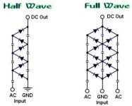
Also it seems that half bridge rectifier is enough instead of the full wave rectifier. So please find attached circuit which uses simple series resonant converter as a current source. Circuit does not need any regulation, since current is function of the supply voltage, resonant pulse repetition frequency and characteristic impedance of the series resonant circuit. So by adjusting pulse repetition frequency you can also change balancing current.

I looked at using a half bridge circuit and it does have the advantage of using half the diodes and high voltage capacitors. The issue I was concerned about was that the return path for the AC drive was through the string of output capacitors, which could be a problem if the cell count was high. Those capacitors may need to be a larger value to compensate.

A constant current drive would be good to limit the current to whatever the diodes can take.

I don't quite follow how driving the circuit off the pack would prevent the cells from being over charged. It's basically the same as a voltage multiplier circuit, so each cell would try to reach the level of the drive. In practice, I would plan on having each cell circuit equipped with an active switch that disconnects the balance source when the cell reaches target voltage. As more cells reach target, the balance current would be directed to the remaining low cells. Eventually the last low cell would get all the current. This same approach would work with a transformer based system, making perfect current distribution unnecessary.

Also, could you post a slightly higer res. picture of your schematic? I can't read the values you used in the simulation and I don't have a spice program. I simulate circuits in my head, or on a breadboard.

One other thing is there tends to be some ringing in the drive from wire inductance. This tends to drive up the voltage on the output caps under light load. With the active cell circuit, this isn't a big problem.

One of the attractions of the capacitor coupled circuit is all the parts could be very small compared to a transformer version.

From http://www.rmcybernetics.com/projects/DIY_Devices/homemade_voltage_multiplier.htm[/attachment]
 

Attachments

  • voltage_multiplier_schematic_diagram.jpg
    voltage_multiplier_schematic_diagram.jpg
    15.7 KB · Views: 2,287
fechter said:
Also, could you post a slightly higer res. picture of your schematic? I can't read the values you used in the simulation and I don't have a spice program. I simulate circuits in my head, or on a breadboard.

Please find larger picture attached. Also, if you wish, you can open schematic attached to my previous post (.asc file zipped) in it' s native spice program. It is free LT Spice IV program downloadable from Linear Technology site. http://www.linear.com/designtools/software/ltspice.jsp

Free does not mean that it is hampered in any way, it is comparable or even superior to other spice packages, only attached library of elements is rather small. But for visualizing circuit operation for us elderly not so fond of breadbording any more it is invaluable tool. I was able to come from your original schematic which I even falsely interpreted to the one I posted in about 1 hour with maybe 5 or more steps in between.

fechter said:
I looked at using a half bridge circuit and it does have the advantage of using half the diodes and high voltage capacitors. The issue I was concerned about was that the return path for the AC drive was through the string of output capacitors, which could be a problem if the cell count was high. Those capacitors may need to be a larger value to compensate.

Ha, now I understand your original schematic (It's a dot thing on junctions and crossings, it is different in Europe and US). I originally thought those output caps were somehow floating.

Yes using output capacitors would be a good thing. But I do not think size would be so problematic. They only see cell voltage. Low ESR capacitors like ceamic MLC , polymer Al or polymer Ta are rather small. In my simulation I do not use them since cells are modeled with 10miliF capacitors to speed up the simulation.
I also used large 100uF AC coupling capacitors in my schematic to speed it up. Otherwise something smaller in the range of the few microF would probably suffice, especially if AC driving source could be run at a higher frequency. I think somewhere around 400kHz would be realistically possible.


fechter said:
I don't quite follow how driving the circuit off the pack would prevent the cells from being over charged. It's basically the same as a voltage multiplier circuit, so each cell would try to reach the level of the drive. In practice, I would plan on having each cell circuit equipped with an active switch that disconnects the balance source when the cell reaches target voltage. As more cells reach target, the balance current would be directed to the remaining low cells. Eventually the last low cell would get all the current. This same approach would work with a transformer based system, making perfect current distribution unnecessary.

As FET half bridge on the schematic is a current source, most of it's current is diverted into the cell with the lowest voltage, and so on. When all cells reach the same voltage, each cell is charged with 1/N current of the current source. But since current source is supplied from the pack and it's efficiency is less than one, it is at the same time discharging the pack with a larger current 1/(N x efficiency), so without external charger with charging current higher than balancing current there is no way to get single cell charged higher than pack voltage /N. (N is the number of cells).

Also, there is a difference between voltage multiplier and your circuit. In voltage multiplier AC driven capacitors are series connected while in your circuit they are parallel connected and essentially function as a DC blocking ( AC coupling) capacitors.

fechter said:
One other thing is there tends to be some ringing in the drive from wire inductance. This tends to drive up the voltage on the output caps under light load. With the active cell circuit, this isn't a big problem.

With resonant converter, driving voltage is not square wave any more but a little more funny looking. There is already inductor in series with the coupling capacitors so some additional wiring inductance should not pose a problem.
 
I've been trying to keep occupied on something decent like simulating circuits, so here is what I've come up with, mainly pertaining to MOSFET drive. I've gotten the rectifier diode configuration (i like it!) from krneki, it is what I was trying to think of doing, just one diode for charging and one for discharging each capacitor. (I get fatigued doing things in real life, kind of like what krneki mentioned, but the simulator is pretty relaxing.)

Fechter was looking for discrete drive and level shifting, something I often use in real life, not just on the simulator. So I tinkered with it on the simulator and got the theoretical timing and the functionality of the high side and low side pretty close.

Edit: using just two diodes for each cell, that is how I use a charge pump to charge the controller power supply capacitor for an offline switcher, but at 60Hz.
 
Beautiful. You've got me sold on LTspice. Breadboarding IS a pain in the ass, but I really trust it more than a spice model in the end. If the spice model allows several iterations of 'corrections' before it goes to hardware, I can see how that could speed things up. Of course I'm new to it and there's a learning curve, but I understand the basic principles.

OK on the not overcharging. At least from an energy standpoint. An individual cell could still go over the desired set point if it no longer presented a load (fault condition). In my application, there would always be power feeding it until the pack was full.

I see how the inductor on the output of the drive will help. It seems like there should be a nice off-the-shelf switching controller chip that I can just set for a given maximum average current such that if all the power goes to a single cell, the diode doesn't overheat. Some kind of current mode synchronous buck converter something or other. There's almost as many of those as there are capacitors :shock: I don't really want discrete drive, in fact, I'd like it if everything was all packed onto a single chip.

I'm still not completely sure about the half bridge for a long string (16+ cells). I think it might be OK if the properties of the cells allow them to act like very large capacitors with low ESR. What does a typical cell look like at 100khz or 400khz? This would be easy enough to test once I get a driver that works well. I think it would be less of a problem at higher frequencies, but then again, packs can be configured in all sorts of non-linear configurations, some of which could look pretty inductive.

While 400khz would be good to minimize the needed capacitor size, it could be challenging to funnel that power into a load if it's very far away. Board layout would need to minimize the path lengths for the high frequency stuff. I also worry about EMI.
 
Thanks. Cool about LTspice. I wish that I had it for playing with electronics circuits instead of frittering away time playing Bards Tale on a Commodore 64 a quarter century ago!

Those are some good musings, especially the question about the high frequency behavior of a cell. I have wondered something like that, too. EMI is an important consideration as well.
 
OK, so after thinking about it some more, I don't see any reason not to use a half bridge. Since one of the major limiting factors will be diode heating, getting rid of one series diode in the ouput will cut the heating in half. It will also give a 'stiffer' output which should improve current distribution. The available selection of Schottky bridges is pretty slim too. Singles have a much better selection and availability.

If there turns out to be a problem with the return path through the cells due to cell impedance at the operating frequency, a second capacitor on each cell tap can provide the return path just like in the full bridge setup. Of course it would be nice to not need them, but if their ESR is low enough, it won't really hurt. It might help keep RF on the board too and not circulate it out to the cells. If the output filter caps on each cell circuit are large enough such that all of them in series still works out to near the coupling capacitor's value, then the return path can be through them and we don't need the extra return path caps.

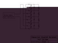
In the schematic below, I also show a 'compensated' feed arrangement. In practice, it might not matter, but if you have a linear arrangement of cell circuits fed by a common bus, if the bus is fed from opposite ends, the path length for each cell is equal, which will compensate for any wire resistance, and similary the total capacitance for each path should be nearly equal.
CCB half bridge with compensated feed.jpg

So back to that pesky driver...

Running it directly off the pack could be an issue at higher voltages. You need a voltage regulator for the control circuit anyway, so I think if I can make it run off something like 12v, getting a 12v supply to handle it will be fairly easy. The 12v can come from a dc-dc that runs off the pack.

If we use an inductor in series with the output, it should be possible to control the current by varying the duty cycle, allowing construction of a constant current source. I don't see any reason the waveform needs to be a square wave, in fact if it was more sinusoidal, there would be a lot less potential for harmonics, ringing and EMI to develop.
 
i found

http://www.instructables.com/id/Switch-mode-LED-torch/

they use a switching pwm driver i wanted to post for anyone to see if it would work for this.
 
I don't think that one will work.

But there are plenty of them out there that look like they would. Too many, in fact. Hundreds, maybe thousands of different ones.

So far I found a few that are good candidates.
Ideally, I'd like one with integrated switches that can do somewhere between 2A - 4A.
A synchronous buck converter is the right configuration.
Adjustable frequency might be nice.
It should be in a package that I can hand build (BGAs look tough).
It should be able to take in input voltage up to 15v or so, but maybe 5.5v might work.
 
My thought on a half-bridge driver would be to use an integrated Half-bridge chip. Infineon makes many different versions for automotive applications. Digikey TDA21201-P7IN-ND also looks interesting and is in stock at Digikey.

I like the simplified schematic you've posted. I'd personally skip the per-cell bypass capacitors and just use the parallel capacitors to ground.


Lawson
 
fechter said:
I don't think that one will work.

But there are plenty of them out there that look like they would. Too many, in fact. Hundreds, maybe thousands of different ones.

So far I found a few that are good candidates.
Ideally, I'd like one with integrated switches that can do somewhere between 2A - 4A.
A synchronous buck converter is the right configuration.
Adjustable frequency might be nice.
It should be in a package that I can hand build (BGAs look tough).
It should be able to take in input voltage up to 15v or so, but maybe 5.5v might work.


i like the idea of a wide voltage range so it can be powered from 3.3 or 5 volt outs on a pc power supply to a car battery.

i say pc power supply because if you ever tore apart an old computer you will see that the the 3.3 and 5 volt rails can put out dozens of amps.


car battery because we can then connect to one of them booster packs used to jump a car or charge on the road.


maybe even be future proof for when hydrogen fuel cells come to market for consumers .
 
lawsonuw said:
My thought on a half-bridge driver would be to use an integrated Half-bridge chip. Infineon makes many different versions for automotive applications. Digikey TDA21201-P7IN-ND also looks interesting and is in stock at Digikey.

I like the simplified schematic you've posted. I'd personally skip the per-cell bypass capacitors and just use the parallel capacitors to ground.


Lawson

Thanks for that. The Infineon chip is pretty nice. It's about half the driver circuit in one package.

Most of the integrated half bridge diodes are common cathode. I'd need a series pair. They do exist, but selection is limited. Reducing the parts count is always good.

I found several integrated synchronous buck converter chips that have pretty much the whole thing on a single chip. Even more that use external FET switches, which wouldn't be too bad.

The bypass cap on each cell may be necessasry for transient suppression anyway, depending on how I do the cell circuits. I'm always looking for ways to leave parts out, so it would be worth testing. If the coupling caps are big enough, they'll be doing the same thing. Across the cell, there isn't much voltage, so it's easier to use a high capacitance value.

SPICE guys:
can the program show what the waveform would look like after the inductor?
 
fechter said:
SPICE guys:
can the program show what the waveform would look like after the inductor?

Yes the SPICE program will show a wave form after the inductor. The wave form will only be as accurate as your simulation. I.e. all components in a SPICE model are ideal. Parasitic components of the circuit need to be added manually if they're important. (or added via component sub models) Also, component variation isn't modeled unless the operator changes values. Finally, the simulation is solved using a descretised time step, any action in the circuit that happens in less than one time step is lost while actions that take only a few time steps are distorted.

Lawson
 
On the version I have, here is the waveform after the inductor. I've named the circuit node "u".
 

Attachments

  • chgpmpdrive.png
    32.3 KB · Views: 1,102
Awesome. It will be interesting to see how close that is to actual. Looks pretty realistic...

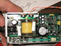
I found a pre-built driver circuit in the form of a half-dead 12vdc to 120vac inverter. This one has a very simple 555 oscillator driving a push-pull transformer. This should be good for some testing anyway, while I continue to shop for a more integrated driver.
 
OK, the junk box yielded an old dc-ac inverter board that still partially worked.inverter board.JPG

This thing has a pretty crude circuit, but it does seem to work well. It uses a center tapped transformer with a pair of FETs in push-pull on the primary. A 555 timer triggers one of the FETs and they both get feedback from the transformer to sustain the oscillation. It makes a pretty even 50% duty cycle, a bit of dead time, and it can handle about 20 amps. I disconnected the secondary winding and just put a pair of wires tapped onto the primary winding that I can run over to my breadboard.

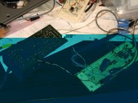
This is what I call GHETTO SPICE.Ghetto SPICE.jpg

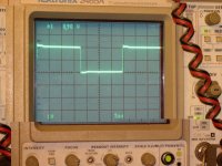
The stock setup seems to be running at around 28khz. Here's the waveform coming off the primary:

The inverter was being powered by 10v. The output seems to be 20v p-p., which is a result of the center tapped primary acting like a 2:1 autotransformer. (Note: I'm using a x10 probe, so actual voltages are 10x what the on screen display indicates)
inverter output.JPG

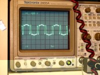
Under load, and after the coupling capacitor, it looks like this:View attachment 3
There's a bit of ringing from all the long wires.

28khz turns out to be too slow for a 4.7uf cap, so I tacked a resistor onto the 555 to speed it up.

Here's what it looks like at about 62khz:inverter at 60khz.jpg

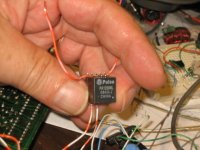
I happened to have some small POE transformers around that I was using for experimentation on a transformer based system.POE transformer.JPG

These are wound at 3.67:1 and can handle about 13W.

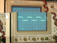
Just for fun, I tried hooking one to the inverter. Here's what it looked like on the secondary:inverter transformer secondary.JPG

Under load, it seemed to behave pretty nicely. I'll have to see what happens if you put more in parallel some day.

I also tested half-bridge vs. full bridge.
 
GGoodrum said:
Man, am I the only one getting a migraine, trying to keep up?? :shock:

-- Gary


I think the only part you need to know, is how purty that waveform of the transformer output looks :) No inductive bounceing nonsense. :)
 
Back
Top