GaN and IMS MESC controller boards

Greeting.
I am very interested in using IMS for power stage but haven't try one yet.
IMO the main obstacles to me seems to be it's hard to router with only one layer but still keeps signal trace away power path.
Would you kindly share and explain your design so that I will learn a lot and made much less stupid mistakes.:giggle:
I thought I explained well and shared screenshots of the layout... Are you asking for the complete KiCAD source files? I'm not planning on publicly sharing them. I'll share them with individuals for personal use, not production and sale.

BTW normally for aluminum PCB, white is the default color for solder mask, did you pay extra bucks for purple?
I didn't recognize it in the first glance. :unsure:
It's a standard 5$ option on jlcpcb. I already made green and black ones so purple seemed worth the extra 2 days turnaround...
 
Last edited:
I thought I explained well and shared screenshots of the layout... Are you asking for the complete KiCAD source files? I'm not planning on publicly sharing them. I'll share them with individuals for personal use, not production and sale.


It's a standard 5$ option on jlcpcb. I already made green and black ones so purple seemed worth the extra 2 days turnaround...
Thanks for reply. I just want some guide. 😋 Here're some of my questions.
First is that some said the gate trace sould not be parallel with the high current trace (e.g. SWx in your example). Could it be a issue? Or when it will be a issue?
The second is did you serial two set of MLCC inorder to get higer voltage tolerance?
Third, I wonder how much current I can get with 1OZ copper IMS. I've heard from somewhere in this forum it may tolerance around 5A/mm before it burst into fire.

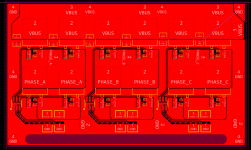
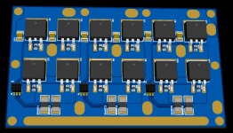
And here's my design. You really inspire me to try this. I hope it will survive form 40-50amps.
top.png
3d.png
 
Thanks for reply. I just want some guide. 😋 Here're some of my questions.
First is that some said the gate trace sould not be parallel with the high current trace (e.g. SWx in your example). Could it be a issue? Or when it will be a issue?
The second is did you serial two set of MLCC inorder to get higer voltage tolerance?
Third, I wonder how much current I can get with 1OZ copper IMS. I've heard from somewhere in this forum it may tolerance around 5A/mm before it burst into fire.

And here's my design. You really inspire me to try this. I hope it will survive form 40-50amps.
View attachment 335967
View attachment 335968
Your design is very close to working well. It will easily handle 40-50A. As long as you choose decent MOSFETs that is.

5A/mm is about right for fr4. On IMS you'll get much more than that.

The double capacitors in my design were because someone was going to put it in a plane and was worried about ceramic cap cracking. Since they massively derate capacitance with voltage... You end up not actually losing much by putting them in series, if anything.

The parallel with high current traces thing. Yes it's an issue but it really isn't here. There's only about 3cm on the board atall and the planes are huge so the coupling is very small.

Actually there's only a few minor things on your board i see might be an issue, 1) no bulk caps. 2) slight imbalance between the two shunts (move them right a tiny bit... Really minor) and 3) maybe add more ground connections to your logic board.
 
Last edited:
Your design is very close to working well. It will easily handle 40-50A. As long as you choose decent MOSFETs that is.

5A/mm is about right for fr4. On IMS you'll get much more than that.

The double capacitors in my design were because someone was going to put it in a plane and was worried about ceramic cap cracking. Since they massively derate capacitance with voltage... You end up not actually losing much by putting them in series, if anything.

The parallel with high current traces thing. Yes it's an issue but it really isn't here. There's only about 3cm on the board atall and the planes are huge so the coupling is very small.

Actually there's only a few minor things on your board i see might be an issue, 1) no bulk caps. 2) slight imbalance between the two shunts (move them right a tiny bit... Really minor) and 3) maybe add more ground connections to your logic board.
Glad to hear your advice. I will come back with some test result in a few weeks.:bigthumb:
 
yes, after-sale support can be daunting but there are some measures you can take to minimize it:

- good and simple documentation, quick-start guides
- pre-configured presets (mostly implemented in software/firmware) simplifying setup
- remote logging to quickly pinpoint and resolve the issue for the customer
- built-in protections mitigating most likely catastrophic scenarios (combination of hw and software protection)

But yes, supplying to a limited number of customers with specific requirements and parameters takes some variables out of the equation.

regarding IMS, we've been using them since 2019 in the NextGen controllers before everyone else jumped on the bandwagon.
Routing high power traces and sensitive gate tracks together on a single layer is more challenging than multilayer FR4 but not impossible. There are few good reference designs available from major electronics companies where it was done successfully. Some additional techniques as snubbers and fast turn off circuits may be necessary to compensate for longer traces. We use multiple protections to ensure switching work predictably and within mosfet specs.

The other big challenge is to make reliable high current connection between the IMS board and power inputs and outputs. Since you can't bolt down current conducting and/or stress-prone elements to the board due to the risk of shorting to the metal layer, there need to be creative ways to attach them reliably to the copper layer. For example, soldering a long phase post direct to the board without reinforcements as done on some IMS using controllers today is likely a bad idea. Thermal expansion needs to be considered when attempting to connect two dissimilar materials such as Aluminum, copper, FR4 for example and tolerances need to be adjusted accordingly. And a lot of other things that may not be immediately revealed at a prototype stage. Reliability issues surface as you start making a product en-mass and testing in with customers.
 
Last edited:
I Googled GaN BLDC controllers and hit this thread. Great job! You mentioned a logic level gate driver that did not mention GaN on its datasheet. Because these use diodes to generate the gate bootstrap voltage, it is not bounded on the upper end. In some situation a little Q can drift in asymmetrically, causing an overvoltage on the EPC gate which have a very narrow range. The mitigation is adding a 5.1V zener across the boot cap.
 
I Googled GaN BLDC controllers and hit this thread. Great job! You mentioned a logic level gate driver that did not mention GaN on its datasheet. Because these use diodes to generate the gate bootstrap voltage, it is not bounded on the upper end. In some situation a little Q can drift in asymmetrically, causing an overvoltage on the EPC gate which have a very narrow range. The mitigation is adding a 5.1V zener across the boot cap.
Thanks for the feedback!

Regarding the zeners and over voltage, it's not a problem I experienced. I was monitoring the gate driver voltage on the high side with a differential probe and it didn't rise above 5V. I do understand the theory of this issue though, and on many of my other boards I've added a zener on the MOSFET gates to clamp reverse voltage and excess positive voltage. If I made another GaN stage (I won't for the foreseeable future; it worked fine but was significantly more expensive than silicon, has that zingy ringing that seems to be innate to the MOSFETs and harder to cool) I would add the zener.

I've actually never had an issue with gate voltage boosting itself too much on any drive I've built, though I've definitely had issues with them going under voltage.
 
Back
Top