Non-silicon and/or soft-switched controller topologies?

ARod1993

100 W
Joined
Feb 24, 2014
Messages
251
Location
Cambridge, MA
I've been lusting after an Emrax 188 for a while; the only concern I have is figuring out how to run it/what controller to run it with. I saw Ben Katz's teardown of the 228LV here: https://build-its-inprogress.blogspot.com/2017/05/emrax-motor-teardown.html and the first thing he mentions is the ridiculously low resistance and inductance (1.12mOhm and 10uH) and a suggested PWM frequency of 100kHz or so to limit current ripple; the only problem is that 100kHz PWM switching is difficult with modern Si MOSFETS.

If we look at the IPT059N15N3ATMA1 (a modern 150V 150A SMT device, datasheet here for reference: https://www.infineon.com/dgdl/IPT059N15N3+G_Rev1.1.pdf?folderId=db3a304326623792012669f6bee2224b&fileId=db3a30433e9d5d11013e9e62778d0185 ) they list turn on time as 35ns and turn-off time as 14ns; if we assume that the switch voltage rise and current drop are linear, you wind up with a triangle whose area is (rise time+fall time)*(peak power per switch)/2. Assuming a 30s pack at 100A per switch, the total loss per switching event is (49ns)(12kW)/2= 294uJ per cycle, which corresponds to about 30W per switch; on a 30-fet controller that translates to 900W of power wasted in switching losses. The I^2R loss per device comes out to (100A^2*0.0059)=60W per device, with a maximum of 1800W in conduction losses, giving about 2.7kW wasted out of 50kW (95% efficiency; not great, not terrible)

In gallium nitride this would be a lot easier to do; the EPC2033 eGaN transistor is also rated for 150V, but has a total gate charge of only 3.2nC (as opposed to the 24nC gate charge required to switch the IPT059N15N3ATMA1 ), which means a 2A driver could conceivably switch them on and off in 1-1.5ns. They also apparently parallel quite nicely, with a positive temperature coefficient. The down side is that they're $8 each, and top out around 30A each, which means for a 450-500A controller you'd need 90-100 devices (which means spending $800 or so on the raw transistors before you do anything else). At that point each device is dissipating (3ns)(120V*30A)/2= 5.4uJ per device, which at 100kHz is 0.54W, or 54W switching loss across an entire 500A controller. Assuming you run your devices at the full 30A all the time, your conduction losses per device are (30A^2*0.007) is 6.3W per device, or 630W total, bringing your total controller losses at 50kW to about 700W (which translates to 98.6% efficiency; much better)

The downside to running GaN in this way is that the power transistors are 4.6mm x 2.6mm 24-BGA dies, and keeping them cool is both important and interesting. The thermal resistance of the GaN dies to the board is 4C per watt junction-to-board assuming each FET gets a square inch of copper board all to itself; if you want to get good cooling performance you could probably push things significantly farther if you mounted a heatsink to the top of the board (they claim 0.45C/W junction-to-case, but then if you use their recommendations for thermal interface materials you get 4.7ish C/W across the top junction, so your total resistance out the top is 5.1C/W. If you use the devices as rated at 30A each that comes out to 6.84W(5.1C/W) or about 30C temp rise above ambient, which isn’t bad. Then it’s a matter of actually driving the FETs, which require a special GaN driver (GaN gates blow through at about 6V, so you need a driver that’s designed to prevent that from happening) that costs about $4 per driver. For a 50kW controller that’s another $200ish of driver chips to make everything work, and laying all this out on a board is going to get really entertaining really fast.

The other alternative would be to use a soft-switched motor driver; they exist and I've seen them in papers, but they're uncommon, wonky, and low power thus far. There's apparently a startup that's commercializing them, but they're actually using an AI to control the preresonant circuit: https://www.electronicsweekly.com/news/design/pre-switchs-soft-switching-power-inverter-2021-04/ I was wondering if any of the old hands on here had any experience with this sort of stuff, and what people's thoughts were on these sorts of controllers?
 
Few comments...
1) I think you might be over estimating the silicon switching losses (you've got an upper bound estimate before allowing for output capacitance and freewheel diode conduction) and under estimating the GaN losses. Switching 500A in 1 or 2ns has some serious implications that it's not clear how you'd overcome them. Ringing for example.

2) centre aligned pwm effectively doubles the switching frequency so 100khz could mean 50khz centre aligned.

3) there's no shortage of companies willing to claim magic sauce to get funding. Until it works and is propelling our cars, or ST, Infineon etc release libraries for it, it's pie in the sky. And when they combine it with "oh we solved it with AI", expect disappointment.
 
mxlemming said:
Few comments...
1) I think you might be over estimating the silicon switching losses (you've got an upper bound estimate before allowing for output capacitance and freewheel diode conduction) and under estimating the GaN losses. Switching 500A in 1 or 2ns has some serious implications that it's not clear how you'd overcome them. Ringing for example.

2) centre aligned pwm effectively doubles the switching frequency so 100khz could mean 50khz centre aligned.

3) there's no shortage of companies willing to claim magic sauce to get funding. Until it works and is propelling our cars, or ST, Infineon etc release libraries for it, it's pie in the sky. And when they combine it with "oh we solved it with AI", expect disappointment.

1) True; if the silicon numbers wind up working out better than that then things are probably pretty good; I'd likely also want to add extra FETs because trying to heatsink an SMT FET is hard unless it's a flip chip die (which the silicon ones aren't). Yeah, the driver datasheet shows closer to 3-5ns when driving one of these; I'm also not sure how to manage the ringing other than doing something clever and skewing the PWM signals within a phase group by a couple hundred picoseconds so that even though each individual GaN device spends no more than 1-2ns turning on the turn-on of the entire phase takes 5-6ns; that would likely also require some fairly clever signal routing. Then there's also the matter of physically arranging everything; the preferred layout for the devices visible in the datasheet is to have VDD and ground as the upper and lower lines on an E, with the center line being the switch node and the gate driver behind the E; that gets harder when each phase has 32 or 34 devices on it (16-17 FETs per leg, one leg to VDD and one to ground).

2) Interesting; I'd never heard of that trick before; we always used edge-aligned in school but in retrospect if that can actually drive down current ripple that might make things work better, which would in turn allow for lower switching frequency and so lower losses :)

3) That's true; the use case is constrained enough that I could believe that AI does what you need it to do here, but I'm waiting to see it actually get used commercially (and would love a soft-switching topology that's closed-form enough that you don't need an AI to get it to work).
 
what about use GaN fets in that soft switch resonant circuit, and as power switch use regular SiC fets ? and drive it paralel ? GaN will switch faster and do fast transition, and then Sic fet will turn on with minimal switching loss...
 
stepus said:
what about use GaN fets in that soft switch resonant circuit, and as power switch use regular SiC fets ? and drive it paralel ? GaN will switch faster and do fast transition, and then Sic fet will turn on with minimal switching loss...

I don't know if that works (but it might); if you're pulling current through a device I would assume you'd have switching losses regardless, but if you were to always close the GaN switches first and open them last the voltage component of your switching losses across the silicon would wind up being something like 2-3V, which isn't bad (though doing that might also do interesting things to the edges of your waveshape).

Another interesting thing to try to do would be to package the GaN dies with a driver into small half-bridge modules and then parallel the modules to produce phase legs of a motor controller; that would basically let you really optimize the switching and driver layout and make providing power much easier. The fun part is going to be actually getting fast edges into the gate driver in that setup; I have a stupid idea that might work if I could find an affordable way to fabricate it. If you feed the gate signal into a stripline with a PN junction as the dielectric you get a varying capacitance that sharpens the pulse as it progresses, letting you extract sharp pulses out of fairly mushy input signals; apparently the technique is a thing you can use to get femto- and picosecond rise-time pulses. Since all I'd need would be <1ns from >5-10ns that should make it easier.
 
ARod1993 said:
stepus said:
what about use GaN fets in that soft switch resonant circuit, and as power switch use regular SiC fets ? and drive it paralel ? GaN will switch faster and do fast transition, and then Sic fet will turn on with minimal switching loss...

I don't know if that works (but it might); if you're pulling current through a device I would assume you'd have switching losses regardless, but if you were to always close the GaN switches first and open them last the voltage component of your switching losses across the silicon would wind up being something like 2-3V, which isn't bad (though doing that might also do interesting things to the edges of your waveshape).

Another interesting thing to try to do would be to package the GaN dies with a driver into small half-bridge modules and then parallel the modules to produce phase legs of a motor controller; that would basically let you really optimize the switching and driver layout and make providing power much easier. The fun part is going to be actually getting fast edges into the gate driver in that setup. I'd probably want to pass the gate drive signals into the half bridges over fiber, and then use a Schmitt inverter to firm up the edges on the received pulse
 
ARod1993 said:
stepus said:
what about use GaN fets in that soft switch resonant circuit, and as power switch use regular SiC fets ? and drive it paralel ? GaN will switch faster and do fast transition, and then Sic fet will turn on with minimal switching loss...

I don't know if that works (but it might); if you're pulling current through a device I would assume you'd have switching losses regardless, but if you were to always close the GaN switches first and open them last the voltage component of your switching losses across the silicon would wind up being something like 2-3V, which isn't bad (though doing that might also do interesting things to the edges of your waveshape).

Another interesting thing to try to do would be to package the GaN dies with a driver into small half-bridge modules and then parallel the modules to produce phase legs of a motor controller; that would basically let you really optimize the switching and driver layout and make providing power much easier. The fun part is going to be actually getting fast edges into the gate driver in that setup; I have a stupid idea that might work if I could find an affordable way to fabricate it. If you feed the gate signal into a stripline with a PN junction as the dielectric you get a varying capacitance that sharpens the pulse as it progresses, letting you extract sharp pulses out of fairly mushy input signals; apparently the technique is a thing you can use to get femto- and picosecond rise-time pulses. Since all I'd need would be <1ns from >5-10ns that should make it easier.
you thing probably something like this but for lower voltage and bigger current, smaller RDSon :D
https://www.st.com/en/power-management/mastergan4.html?ecmp=tt21426_gl_enews_may2021&cid=stmDM42844&bid=422474110&uid=i7MoE6ZPxHsHXz2KH+RCfjGn2fRmi5CJ
 
Yeah; the idea was to use the loose FETs from EPC and the TI driver and build a 200V 30A half-bridge that I could then just tile for more current handling capability. My thought process was two of these:

https://epc-co.com/epc/Portals/0/epc/documents/datasheets/EPC2034C_datasheet.pdf

driven by one of these: https://www.ti.com/lit/ds/symlink/lmg1210.pdf?ts=1622668854312&ref_url=https%253A%252F%252Fwww.ti.com%252Fproduct%252FLMG1210

with either a fiber trigger and an internal Schmitt inverter to firm up the pulse edges, or some other clever connector to isolate gate inputs from switching noise. They even have a recommended four-layer board layout for making half-bridges on page 8 of this whitepaper: https://epc-co.com/epc/Portals/0/epc/documents/papers/eGaN%20FET%20Drivers%20and%20Layout%20Considerations.pdf

I may throw something together in KiCad tonight or tomorrow and see how it looks :)
 
I'm wondering with that gate driver and clever use of the dead time thingy whether you could have say 2GaNfets top and bottom with ultra low inductance switching very fast and a large number of silicon TOLL FETs switching a lot (10x) slower and off sooner/on later in parallel.

Possibly get the best of both worlds. 99% of the time the current is taken by the TOLL FETs with much lower Rds on and the other 1% the GAN FETs are taking the high frequency stuff and providing an 8mohm path while the big TOLLs are partially on with much higher resistance.

I like this idea.

Look into stm32f334. It has a high resolution timer (217ps resolution) with incredible flexibility that could easily drive the big/fast FETs independently if necessary.
 
mxlemming said:
I'm wondering with that gate driver and clever use of the dead time thingy whether you could have say 2GaNfets top and bottom with ultra low inductance switching very fast and a large number of silicon TOLL FETs switching a lot (10x) slower and off sooner/on later in parallel.

Possibly get the best of both worlds. 99% of the time the current is taken by the TOLL FETs with much lower Rds on and the other 1% the GAN FETs are taking the high frequency stuff and providing an 8mohm path while the big TOLLs are partially on with much higher resistance.

I like this idea.

Look into stm32f334. It has a high resolution timer (217ps resolution) with incredible flexibility that could easily drive the big/fast FETs independently if necessary.
My plan for generating the controls thus far was to use an Artix or Zynq (100kHz PWM means I probably want at least 500kHz-1MHz sampling, and it's probably easier to do that if I can do the controls directly in hardware (Clarke/Park transform, PI controller, inverse Clarke/Park, and SVPWM generation could possibly all be gotten done in 3-5us, which would leave room for running 100kHz center-aligned PWM easily (and possibly enable operation up to a few hundred kHz PWM frequency for people who want really tight controls), and then use a uC to process slow things like throttle inputs (current sensors would be directly interfaced with the FPGA).

Driving a combined setup would also be interesting but it doesn't seem too terrible; the big thing would be that there'd likely need to be a second, shorter pulse to drive the Si chips, and the minimum on-time of the whole setup would be dictated by the minimum on-time of the big Si FETs. Also, 200kHz center aligned (100kHz switching losses, 200kHz ripple) should be able to drive most of the really nice motors that turn out to be miserable to work with because low resistance/low inductance
 
Few comments...

You only need 1 sample per pwm period, possibly even only one per several periods. But it needs to be synched well with the pwm to avoid noise.

You only need to run the FOC control loop much less frequently than the pwm. Like often enough to account for changes in motor speed, any more is basically pointless. If you're running it sufficiently fast to account for bad back emf profile, you have to realise that making perfectly sinusoidal current will not reduce torque ripple, since the torque is dependent on the magnetic field which in turn defined the back EMF profile. Running it once per period doesn't harm, but it really doesn't help either (though you absolutely have to update the pwm to account for rotor position every pwm period, and with centre aligned you can update it at the top and bottom mid.

There's no particular reason why at low on time you have to turn the Si FETs on, though they do present a practical limit to your max frequency (they won't be doing anything to help).

I'm not really atall familiar with fpga, but know enough to know it makes generating the pwm and dead times super super easy, and since they are always 3 million pin bgas there's no shortage of pins to interface with... Any number of gate drives
 
mxlemming said:
Few comments...

You only need 1 sample per pwm period, possibly even only one per several periods. But it needs to be synched well with the pwm to avoid noise.

You only need to run the FOC control loop much less frequently than the pwm. Like often enough to account for changes in motor speed, any more is basically pointless. If you're running it sufficiently fast to account for bad back emf profile, you have to realise that making perfectly sinusoidal current will not reduce torque ripple, since the torque is dependent on the magnetic field which in turn defined the back EMF profile. Running it once per period doesn't harm, but it really doesn't help either (though you absolutely have to update the pwm to account for rotor position every pwm period, and with centre aligned you can update it at the top and bottom mid.

There's no particular reason why at low on time you have to turn the Si FETs on, though they do present a practical limit to your max frequency (they won't be doing anything to help).

I'm not really atall familiar with fpga, but know enough to know it makes generating the pwm and dead times super super easy, and since they are always 3 million pin bgas there's no shortage of pins to interface with... Any number of gate drives

Ahhh, OK. I got confused from reading a Lebowski thread where he talked about needing to sample things at at least 2-3 times faster than the PWM waveform in order to get a decent picture of what was going on (I believe he was discussing 20-30kHz sampling rates for 6-7kHz PWM) and I assumed that you wanted to set your system up to react quickly you needed to be oversampling the PWM waveform (the Nyquist limit would require sampling at least twice the PWM frequency, preferably four or five times if you want to be sure), and that all of that would be passed into the FOC loop. I'm guessing there are averaging techniques you can use so that your input bandwidth doesn't include your switching frequency, and then you dump the filtered inputs into your transforms to do controls things with.

And yeah, FPGAs are amazing to work with in terms of what you can do and how fast they run, the caveat is that they're an absolute bitch to lay out because there are so many bloody pins (especially if you're doing high-speed things, which this design may well qualify as), but if I'm trying to do a lot of fast matrix math an FPGA is the way to go (and since a BLDC controller capable of driving an Emrax without exploding runs on a large pile of matrix math running at least 100kHz it's perfect for the application). Basically I want this to eventually turn into a Fast FOCer that can run ridiculous motors, because I want to put an Emrax 188 or 208 on it and then put that setup into a reverse trike frame along with a bunch of batteries.
 
Oversampling on Lebowski I think was for live inductance tracking for sensorless from standstill. He injected a tone at the pwm frequency by phase shifting the phases and using a filter to amplify the high frequency current component, therefore needing to satisfy nyquist for a signal at the pwm frequency.

For FOC, the signal is very low frequency, on the timescale of the speed you can move the throttle or change speed. It's not the pwm frequency since you're doing all your control in the rotor reference frame.

If you're planning sensorless operation you need faster sampling since you're reconstructing the sinwave off the back emf, but that's still far slower than the pwm frequency.

I bet a standard VESC could control an emrax 228. My controller doesn't seem too bothered running a tiny motor with 6.5uH inductance at 35khz pwm, 70khz switching.
 
mxlemming said:
Oversampling on Lebowski I think was for live inductance tracking for sensorless from standstill. He injected a tone at the pwm frequency by phase shifting the phases and using a filter to amplify the high frequency current component, therefore needing to satisfy nyquist for a signal at the pwm frequency.

For FOC, the signal is very low frequency, on the timescale of the speed you can move the throttle or change speed. It's not the pwm frequency since you're doing all your control in the rotor reference frame.

If you're planning sensorless operation you need faster sampling since you're reconstructing the sinwave off the back emf, but that's still far slower than the pwm frequency.

I bet a standard VESC could control an emrax 228. My controller doesn't seem too bothered running a tiny motor with 6.5uH inductance at 35khz pwm, 70khz switching.

Ahhhhh OK, that makes a lot of sense. Though if you don't mind my asking, what voltage is your 6.5uH motor running at? Since V=Ldi/dt, a motor with 6.5uH inductance and 150V bus voltage would see 23amps per microsecond rise, so over a single 100kHz period you'd see something like 230A ripple (whereas at 48V you'd see something like 80A ripple at 100kHz, or about 120ish at 70kHz switching frequency).
 
Good catch. It's running at up to 24V. Beyond that and with a kV of 1100 and 6 pole pairs... It doesn't stand a chance.

Emrax' partners do not supply high switching frequency controllers. Sevcon etc are all through hole to220 silicon. Very basic.
 
mxlemming said:
Good catch. It's running at up to 24V. Beyond that and with a kV of 1100 and 6 pole pairs... It doesn't stand a chance.

Emrax' partners do not supply high switching frequency controllers. Sevcon etc are all through hole to220 silicon. Very basic.

Gotcha :) I want to try my hand at cutting a fast FOCer (though heatsinking is going to be entertaining; at this point I'm thinking of using heat pipes on the half-bridges because you can store so much energy in the heat of vaporization of most liquids and then you don't need to deal with trying to make a manifold).
 
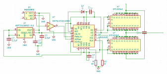
Here's a first draft of the eGaN half bridge design in KiCad schematic:

Fast FOCer half bridge schematic A.PNG

I designed the half bridge to take PWM inputs in over RS422 so that I could bring that in over shielded twisted pair to avoid switching noise on the gate, then a Schmitt trigger inverter firms up the pulse edge to 2 or 3ns (and also flips polarity so that the fail safe value of the RS422 corresponds to low side connected to the motor.
 

Attachments

  • FastFOCer Layout Start.PNG
    FastFOCer Layout Start.PNG
    64 KB · Views: 816
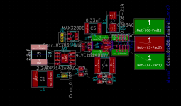
I'm starting to play with laying it out; it looks like each half bridge will wind up around 2"x1.5", maybe a little smaller:
FastFOCer Layout Start B.PNG
I'm trying to follow the layout guidelines from this app note and then referring to this eval board to make sure I'm on the right track; comments and feedback from people with experience doing this sort of layout are greatly appreciated!
 
Few comments...

I think your hs pad and vss pad are mixed up?

No gate resistor footprints. TI seem to be using 0201 0ohm. I'd be inclined to fit the footprint.

Try to get some smaller package high voltage caps to decouple the bus voltage and ground super close to the chips, even if only a few nF. Going through the board probably has significant inductance. I know TI does it with a moderately big loop, but you can see the consequence of that even in their own appnote you linked with big spikes on the vdd line, which ultimately reduces your FET headroom.

Quite cool that it looks like you're actually going to do this!
 
mxlemming said:
Few comments...

I think your hs pad and vss pad are mixed up?

No gate resistor footprints. TI seem to be using 0201 0ohm. I'd be inclined to fit the footprint.

Try to get some smaller package high voltage caps to decouple the bus voltage and ground super close to the chips, even if only a few nF. Going through the board probably has significant inductance. I know TI does it with a moderately big loop, but you can see the consequence of that even in their own appnote you linked with big spikes on the vdd line, which ultimately reduces your FET headroom.

Quite cool that it looks like you're actually going to do this!
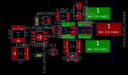
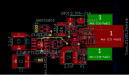
Thanks for the advice and encouragement! I fixed the issue with the HS and VSS pads and added a bunch more capacitance; two 22nF and two 220nF 250V 0805 X7R capacitors directly under the transistors and gate driver on the back side of the board (there's 4.4uF 250V X7R on the backside under the switching node output pad as well). I also tweaked the bypass caps on HB/HS and VDD/VSS; there's now 22nF super close to the chip (1-2mm out from the pads in question) backing up the 2.2uF bypass caps. I'm going to take a nap before the morning, but here are some images of how far things have gotten:

Top side of the board looking down:
FastFOCer Layout Start C.PNG

Bottom layer of the board, showing bus voltage, bus ground, and bypass caps(4.4uF between the board connection pads, 44nF right under the gate driver, and 440 nF under the transistors:

FastFOCer Layout C BackSide.PNG

I still need to the do the rest of the power planes under the GaN devices and then finish up the left side of the board (which is basically all signal and auxiliary stuff). I set it up to take RS422/RS485 commands for PWM because I can send that over shielded twisted pair, and since it's differential the bus EMI shouldn't make things turn on. I put a Schmitt inverter on the output of the RS422/485 receiver, which does two things; it firms up the output edge so that the gate driver should see clean 2-3ns edges coming in, and it means the bus failsafe signal is low (so if something stupid happens the switching node is grounded rather than floating at voltage. I also added a little SOT23 LDO to power the inverter and the RS485 receiver; that way each half-bridge only needs to take in bus voltage, bus ground, an RS422/RS485 signal, and a 6-7V auxiliary input to drive the gate driver and 5V circuitry. All the parts in here that see bus voltage are good to 200V or more (the transistors and driver are good to 200V, the caps are good to 250V and X7R rated, and the bootstrap diode is good to 650V (because this was actually a smaller package than the 300mA 300V diodes on Digikey.

If you only wanted to run this to 140V (probably a 30S pack would be the limit though because bus ringing and voltage overhead) you could just use an LTC3638 switching supply to make the 6-7V auxiliary rail, and then the half bridge would literally only need bus voltage, ground, and an RS422/485 input, but the power supply is $10 from Digikey (and by the time you add the rectifier diode and the inductor and low ESR output caps you're at a $20-30 supply). Since the modules are probably about $40-50 BOM in quantity one, and $25-30 in quantity 50-100 adding that cost per module makes no sense.

All told, the BOM cost of a 60-80kW Fast FOCer would probably come in about even with an Emdrive 500 or a Unitek Bamocar (500A current handling with reasonable overhead would be 17 of these half bridges in parallel per phase, which is 102 transistors at $5.68 each plus 50 gate drivers at $4.59 each plus 250ish $1.50 capacitors, which comes to about $1200 already). Add in nice high-bandwidth current transformers, PCB assembly costs, the FPGA, and all the miscellaneous hardware you need to package this up and you'll probably wind up close to $2-3k BOM cost. The nice thing about having it be modular like this though is that you only need to pay for the power you're planning on using, so a 50-60A controller would only need six half-bridges, plus the GaN setup buys you about 3-5% more efficiency at 100kHz and probably enables up to 1MHz PWM if need be.
 
Use the trace clean up tool. You've got traces clashing with each other and even shorting out a cap.

Pretty sure you don't need such huge caps c4 c5... The big caps are only needed on the bus rails.

Try displacing the MOSFETs 1 pitch left/right so the switch nodes are in line. Phase connection above not to the side.

Have an electrolytic on the bus. Not because it's needed as a buffer at that frequency, though it'll help a bit, but because the esr provides some damping.

Last comment is that having 3 seperate u v w phase drivers isn't really a good thing, since they interact with each other, and are being switched between power and recirculation very quickly. 100k times a second, your switching from:
current recirculating through the high sides, to
Powered 2 phase connected high 1 connected low to
Powered 1phases high 2 low to
Current recirculating on the low side to
2 low 1 high to
1 low 2 high
Repeat

The loops between the phases vbus and ground are very important as well otherwise your capacitors will be absolutely hammered and your ground stability will suffer.
 
Thanks for the advice! I'm gonna take another crack at laying things out when I'm more awake; my questions and comments are in italics below:

mxlemming said:
Use the trace clean up tool. You've got traces clashing with each other and even shorting out a cap.

Pretty sure you don't need such huge caps c4 c5... The big caps are only needed on the bus rails.

Those came from the datasheet for the LMG1210; they have a formula for the bootstrap capacitor sizing based on the maximum on-time for the high-side FET; I designed this in a flash of inspiration last night so I may want to recalculate to make sure I calculated for 10us and not 100us because tired. They also recommend the VDD-VSS cap be at least 5 times the bootstrap cap size so that it doesn't pull VDD down and out of regulation

Try displacing the MOSFETs 1 pitch left/right so the switch nodes are in line. Phase connection above not to the side.

Good idea, thanks!

Have an electrolytic on the bus. Not because it's needed as a buffer at that frequency, though it'll help a bit, but because the esr provides some damping.

Same, thanks!

Last comment is that having 3 seperate u v w phase drivers isn't really a good thing, since they interact with each other, and are being switched between power and recirculation very quickly. 100k times a second, your switching from:
current recirculating through the high sides, to
Powered 2 phase connected high 1 connected low to
Powered 1phases high 2 low to
Current recirculating on the low side to
2 low 1 high to
1 low 2 high
Repeat

Could you elaborate on what you mean by three separate U V W phase drivers? I decided to make half-bridge modules because they seemed like the easiest way to address EMI issues from switching GaN at the relevant power levels and frequencies; there may be better ways to trade that off but this is my first time laying out a real board and so I'm a bit paranoid :)

The loops between the phases vbus and ground are very important as well otherwise your capacitors will be absolutely hammered and your ground stability will suffer.
 
So regarding the caps, it might be the voltage you're over rating. The gate driver caps (low and boot strap) don't need to be rated for the bus voltage, they only see 12V or whatever your gate driver supply is (5 for GaN?)

The motor phases are traditionally labeled U V W. No idea why. Each motor phase is connected to a half bridge.

Consider low speed high current. 10% duty 500A

90% of the time the motor is freewheeling the current, the phases are unpowered but shorted together through the bus or ground planes.

100k times a second you're swapping this path... Several times...

The ground and vbus links between your half bridges have an inductance. If you're using discrete wires and they connect at the power connector, that inductance could be up to about 1uH. So you're switching 500A between 1uH paths in 2-3ns,100k/second.

That is a very big EMC weapon and some serious ground plane bounce/voltage spikes.

The appnote you have is for a dcdc converter where there's only 1 half bridge so this is much less relevant.
 
mxlemming said:
So regarding the caps, it might be the voltage you're over rating. The gate driver caps (low and boot strap) don't need to be rated for the bus voltage, they only see 12V or whatever your gate driver supply is (5 for GaN?)

The motor phases are traditionally labeled U V W. No idea why. Each motor phase is connected to a half bridge.

Consider low speed high current. 10% duty 500A

90% of the time the motor is freewheeling the current, the phases are unpowered but shorted together through the bus or ground planes.

100k times a second you're swapping this path... Several times...

The ground and vbus links between your half bridges have an inductance. If you're using discrete wires and they connect at the power connector, that inductance could be up to about 1uH. So you're switching 500A between 1uH paths in 2-3ns,100k/second.

That is a very big EMC weapon and some serious ground plane bounce/voltage spikes.

The appnote you have is for a dcdc converter where there's only 1 half bridge so this is much less relevant.

Ahhh, that makes sense; I went 250V X7R for all the caps on that board because I assumed I'd need that, but at 12 or 15V X7R I can probably drop a fair number of those capacitors down to more reasonable package sizes. And yeah, getting the layout for the three phases is going to be interesting. My current idea is to mount each of the small half bridges on either another PCB or (more likely) on internal busbars (power and ground busbars on the bottom, phase busbar on the top) to try to drive down internal bus inductances (also busbars are great for mounting bulk capacitance across)
 
mxlemming said:
So regarding the caps, it might be the voltage you're over rating. The gate driver caps (low and boot strap) don't need to be rated for the bus voltage, they only see 12V or whatever your gate driver supply is (5 for GaN?)

The motor phases are traditionally labeled U V W. No idea why. Each motor phase is connected to a half bridge.

Consider low speed high current. 10% duty 500A

90% of the time the motor is freewheeling the current, the phases are unpowered but shorted together through the bus or ground planes.

100k times a second you're swapping this path... Several times...

The ground and vbus links between your half bridges have an inductance. If you're using discrete wires and they connect at the power connector, that inductance could be up to about 1uH. So you're switching 500A between 1uH paths in 2-3ns,100k/second.

That is a very big EMC weapon and some serious ground plane bounce/voltage spikes.

The appnote you have is for a dcdc converter where there's only 1 half bridge so this is much less relevant.

My plan is to mount the half bridges directly on copper busbars (1/4" x 1/4" cross section should work) with a load of additional capacitance mounted directly to the back side of the busbars (a few uF stays on the half-bridge itself for hyperlocal buffering, and then a millifarad or so of mixed film/electrolytic per half bridge on the back side). According to the Internet, a 1-foot length of 1/4"x1/4" bus bar has about 175nH of inductance, and 1/2" x 1/4" bus bar has about 100nH or so. Add several millifarads of capacitance to the bus and you'd get the bus resonant frequency down to around 20-40kHz (or less than half the PWM frequency). I'd be tempted to use something similar to gang the half bridges on the phases together, and then terminate it in something wide enough to take a 3/8-16 screw (I figure 3/8 lugs should fit on 1/0 and 2/0 cables, and for the currents this is going to pull I'd want to go that large to minimize wire drop)
 
Back
Top