YAFO- Yet another FOC controler

GetItFix

1 mW
Joined
Sep 23, 2023
Messages
13
Location
Europe
Dear All,

I would like first to thank all the members on this forum who shared their knowledge on FOC control design.
Finally, after investigation around MP2-ESC, Cheap FOcer, A200S, and other VESC-compatible HW, I have decided to design my ESC with the following constraints:

- Reliability/Robustness on top priority
- 14s Battery
- 50 Amps per phase
- TO 220 FET's
- Classic 8 pin drivers for each leg.
- Ease of DIY soldering AND servicing.
- No fine pitch components, except MCU (no choice !)
- Running VESC FW compiled with the appropriate parameters set
- Full compatibility with VESC tool
- 4 layer design PCB
- HAMMOND 1490WB Aluminum enclosure (106mm x 54mm pcb size)


So, here is the first draft of the schematic and any feed back will be welcome.
 

Attachments

  • Yafo_1450_v0.pdf
    1 MB · Views: 51
One thing I dont like is the D40. Maybe replace it with a <10 Ohm resistor, reduceing the peak voltage stress instead of keep the peak voltage.
And why you connect the snibber to +BATT instead of the Phase_x?
 
Thanks for this feedback
One thing I dont like is the D40. Maybe replace it with a <10 Ohm resistor, reduceing the peak voltage stress instead of keep the peak voltage.
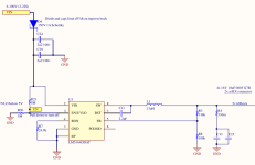
I have used the same input circuitry which is used on the TeamTriforce A100S. (see picture)
Therefore, I think that I will keep the diode and will add a resistor of about 0.5 Ohms in serial with it.
1695743007842.png

And why you connect the snibber to +BATT instead of the Phase_x?
I do not plan to use snubbers on this 50 amp design, may be yes on a bigger one.
But you rise a good question:
I have seen snubbers between +BATT and phase_x (ie. CheapFocer 2) ...
...and I have also seen snubbers between +BATT and GND (ie. BESC Gen 2)
So, what is the optimal solution ?
 
Last edited:
Hi All,
Here is a small update of the schematic where I have added a 1R resistor before D40 diode, according to hbozyq suggestion.
I have also changed current shunt resistor from 0.4 to 0.33 milliOhms, allowing a current read of +/- 100 Amps
Then, last but not least, I have included in the schematic the following figure which shows some open hardware VESC-compatible projects on this forum. There is an exception with the A100S (commercial product) because I found the schematic on the net.
Please, feel free to make comments/corrections/updates if needed.

1695927102266.png
If the schematic doesn't show major errors, then i will start the pcb routing 🤪
 

Attachments

  • Yafo_1450_v0.pdf
    1.1 MB · Views: 6
Last edited:
This will work I think. Looks sensible for a simple controller. I'm always an advocate for hardware over current and also increasingly like gate drivers with enforced anti shoot through time. This is because I've seen some weird things on startup recently.

The canonical VESC hardware is the 75300. It's not the best in every way, but it and the VESC 6 and 100250 is the hardware Benjamin bases his development work on so if you want it to work well, keep your connections and filter constants similar to that.

Leave provision for parallel gate capacitance, and perhaps Diode resistor fast turn off. But don't populate them unless absolutely needed.

Consider fd6288q gate driver for 6 fet design. Save you space and has shoot through prevention and better voltage rating. The ucc part you listed is a bit hair trigger and allows shoot through and it's marginally rated for higher cell count application.

The numbers you've cited for the ESCs in that list are quite conservative. If people ran then at those powers they would probably last ages, but they don't. They get immediately jacked up to twice those numbers by most users.
 
Thanks mxlemming for your reply.
The ucc part you listed is a bit hair trigger and allows shoot through and it's marginally rated for higher cell count application.
Do you know others half bridge drivers preferably from TI, Infineon, Fairchild, ST and so on that could do the job ?
May be should I use a UCC27714 rated for 600 V but it will need an external bootstrap diode and gate pull down resistors.
In addition to this, this one has 14 pins instead of 8. And still no shoot-trough prevention.


I'm always an advocate for hardware over current and also increasingly like gate drivers with enforced anti shoot through time. This is because I've seen some weird things on startup recently.
Understood. Safety by hardware often better than SW. If I go for that, Il means that VESC firmware should take into consideration a special input on the MCU (similar to PB12 on your pill design) to reset all PWM outputs.
I did not found that option in the VESC source code.
Another alternative could use a driver with a ENABLE input connected to the output of current comparator.
Even with this 100% hardware solution, the MCU must be informed that "something went wrong" in order to take appropriate action.


The canonical VESC hardware is the 75300. It's not the best in every way, but it and the VESC 6 and 100250 is the hardware Benjamin bases his development work on so if you want it to work well, keep your connections and filter constants similar to that.
The 75300 has some kind of programmable filter with two possible choices 1k/1nF or 1K/15n. I have chosen a fixed one with 1k/1nF.
Do you think I should keep these values ?
 
Last edited:
Thanks for this input. I am now routing the pcb and I need some advice regarding the use of vias on the gate circuit path.
First of all, my intention is to go for a 4 layer stack-up with Signal/Power - Ground - Ground- Signal/Power as explained here
The idea behind this is to leave the power traces outside with locally soldered copper strips.
I have also physically separated power ground and signal ground on front layer and connected them only in one point.
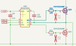
So here is the schematic portion showing the gate current path on the hi-side
1696323273039.png

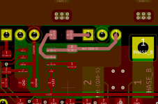
Now, I have 2 possible options for the gate path. Here is the first alternative for the routing:
1696323653513.png

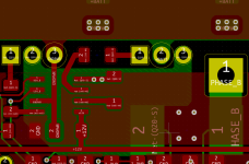
And the second alternative using two vias from front layer (red) to back layer (green)
1696323789528.png

So, any comment and suggestions will be welcome !
 
I really like these gate drivers 2EDF7275KXUMA1
This is a really good driver. I use them.

Thanks for this input. I am now routing the pcb and I need some advice regarding the use of vias on the gate circuit path.
First of all, my intention is to go for a 4 layer stack-up with Signal/Power - Ground - Ground- Signal/Power as explained here
The idea behind this is to leave the power traces outside with locally soldered copper strips.
I have also physically separated power ground and signal ground on front layer and connected them only in one point.
So here is the schematic portion showing the gate current path on the hi-side
View attachment 340436

Now, I have 2 possible options for the gate path. Here is the first alternative for the routing:
View attachment 340437

And the second alternative using two vias from front layer (red) to back layer (green)
View attachment 340438

So, any comment and suggestions will be welcome !
First one preferable. Kelvin connected.

Biggest issue lack of obvious decoupling capacitor.

Look at the mp2 /F405 pill repo, the pb12 code is in the hardware conf .c and .h

It's handled in hardware on the stm32... once the MCU has run the boot code, the timer has dedicated circuits to implement the brk. There's no MCU core involvement and it trips in less than 1 clock cycle.
 
First one preferable. Kelvin connected.
OK, mxlemming I followed your suggestion. Thanks for this valuable input.


Biggest issue lack of obvious decoupling capacitor.
I have put 5 x 2.2 uF 100V MLCC caps on the pcb backside, close to the FETs. (items C90 to C94)
May be 2.2 uF is not enough and should I change for more ?

1697297862295.png


Look at the mp2 /F405 pill repo, the pb12 code is in the hardware conf .c and .h
Yes.This give me some hardware improvement for the next version with external over-current protection, like you did with MP2
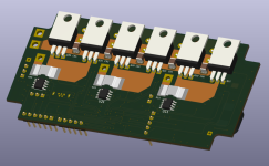
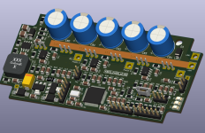
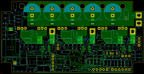
For the time being, this very first release look like this:
1697298572963.png

Now comes some DRC checking and then the boring tasks like components reference selecting and ordering...
 
Last edited:
2.2u is enough. Through hole FETs limit the surf you can switch and your bulk caps are close as well.

Your say you have physically separated the grounds except attachment at one point. How is this affecting your low side gate drive? Or have you made the classic mistake of assuming the signal between the MCU and gate driver can work fine with terrible ground connection?
 
Thanks for this positive questioning.
Your say you have physically separated the grounds except attachment at one point
Yes Sir. That was based on my previous job on single phase induction heater controls, based on IR2113 drivers. (230 VAC up to 7 kW)
I have followed 4 basic rules for power stage design I learned in the university:

1- Put drivers as close as possible to the MOSFETS​
2- Use two planes for power ground / signal ground, and connect them on a single point when dealing with high amps path.​
3- Add a tank cap AND a decoupling capacitor close to each driver VDD's . The "AND" is very important.​
4- Add one or two uninterrupted ground planes​

Of course, there are also others rules to follow, but these 4 ones became familiar for me.
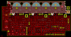
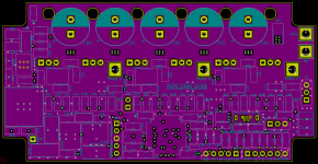
So, here is the front planes with PWRGND and GND.
Connection between these planes are on the top left side through R0 resistor, which will be a solder bridge in the real world.

PWRGND Plane, front layer
1697472758256.png
GND Plane, front layer
1697472809980.png

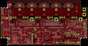
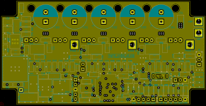
For information, here the back layer showing the power trace +BATT , phase shunts and phase planes
1697473374471.png

GND plane, Inner layer 1.
1697474014080.png

GND plane, Inner layer 2
1697474077083.png
 
Hi All,
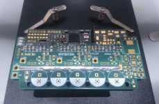
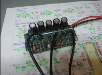
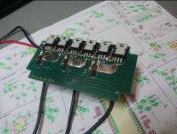
Got the pcb. Now time for manual soldering 😥
Very fine tip, soldering flux and controlled temperature iron are mandatory.
Job will start by the inner/lower components and then going outside.
1698334849166.png
Surprisingly, the main difficulty was not the STM32 chip but the very small ferrite beads. I think I have reached my limits here.
STM32F405
1698335014218.png

Ferrite bead (really ugly, but cannot do more)
1698335077738.png

To be continued....
 
Probably a bit late now but when bringing up a board O always solder DCDC first then the consumers of power so I can test the voltage rails before putting the hours in to add the tricky stuff and expensive stuff. Too easy to wreck everything on a board with a converter error.

Your soldering looks better than mine tbh
 
Last edited:
Hi all,
Back to home and back on the project too !
PCB is now ready. 100 % hand soldered.
Started to test DC/DC conversion stage with a 0-60 Vdc current-limited lab power supply.
In the mean time, downloading and installation of VESC tool 6.02 on a linux laptop...

1701330966817.png

1701331015975.png
To be continued...
 
Last edited:
Following Testing OK:
At 60 Vdc I got a stable 3.3 V on the CPU.
I also write a very basic sketch to blink alternatively the green/red leds
Downloading the sketch using ST-Link working
Test program running OK with led blinking
 
Binary code ready with 2 customized files in /hwconf/other.
Other firmware code files left unchanged. Build firmware is 6.05
Flashing yafo_1450.bin using ST-Link.
Power off / Disconnect ST-Link / Connect usb cable / launch VESC tool / Power on board / click on connect in VESC menu
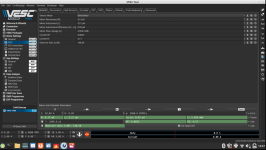
USB Communication between yafo board and VESC tool established
1701336031058.png

To be continued...
 

Attachments

  • hw_yafo_1450.c
    7.4 KB · Views: 2
  • hw_yafo_1450.h
    9.5 KB · Views: 1
Last edited:
Got limited mode with VESC tool 6.02 and firmware 6.05. Still learning.
Downgrade to ground firmware ver 6.02
Recompile
Flash binary
Start FOC Autotune.
Got Happy

1701763332587.png

To be continued...
 
Hi All,
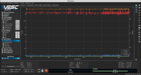
I have a tricky problem with displayed Amps vs real Amps:
Here are the test conditions:
Custom hardware/firmware using the above hw_yafo_1450 custom files.
FOC detection parameters done.
10 poles motor at no load running very well up to 60000 ERPM in FOC mode.
ADC Throttle as input.

14s battery and 1.20 A drawn from battery but more that 15 Amps displayed on the VESC tool !
About less that 2 amps really measured on motor phase using a current clamp multimeter.


1702654694291.png

Of course, I have double checked the INA240 Gain and shunt resistors (50 and 0.3 milliOhms here) in the above files.
Any input will be welcome !
 
Back
Top