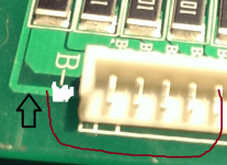
we did something like that but what you can do is solder those two sense wire pins together there where the solder pads are in your second picture.
that will bypass channel #1 and make the B1 pin become the new B- pin and it will then be connected to the B- spot up in the corner where the battery ground is soldered to the pcb.
for the circuit current voltage you can go look on the back side and see where there is a trace coming from the top of #3 and it runs over to the where the thermal breaker is soldered into the pcb. when you find that trace. look at it so you can grasp what it is that it does. the circuit current comes from the top of #3 and goes through that trace to the thermal breaker. from the thermal breaker it goes on to the gate drivers for the mosfets.
so when you bypass channel #1, the voltage that the circuitry uses is now only 2 cells high in voltage so at the LVC, that can be as low as 5.4V and that is too low to be safe for driving the mosfets.
so now you wanna go find the pad at the bottom of the shunt resistor for channel #5 since that will be the top of channel #4. it is easier to solder there to the bottom of the resistor, and you can see where the trace runs down to the B4 pin. that is where you wanna take off the circuit current for this new setup.
i did not see the wires for the 9 pin plugs i installed on that BMS in your picture either so you could solder the wire for the new circuit current there, except it is really hard to solder to them without shorting them.
but you still have the trace running from top of #3 over to the thermal breaker. if you unsolder the leg of the thermal breaker there, you can put a switch in the middle between the top of #4 and that wire to the thermal breaker, and the top of #3 is now no longer in contact with the thermal breaker since it is pulled out of the via.
so now you will have current from the top of #4 going through the switch, into the breaker and then it goes on to the mosfet drivers.
so now you will have a 23S BMS, but your sense wires are all now connected to the wrong cells. they will each have to be unsoldered and moved DOWN one cell, and the B- wire is now excess. so the top of channel #24 is now connected to the top of cell #23.
make sense? i would still like for you to verify that the Q1 is dead. instead of using the continuity tester, please use the diode tester function on your voltmeter to test the body diode of the shunt transistor mosfet. measure between the drain and the source, and show that it is shorted in both directions, compare the forward bias to the adjacent mosfet to prove it is defective. then test the gate to source with the diode tester by applying the probes to the gate and source and the gate and drain to prove it is shorted and how much in each direction.


