VESC based +200A powerstage with 200V MOSFETs (videos of it in action)

zombiess

10 MW
Joined
Jan 31, 2011
Messages
3,048
Location
Oklahoma City
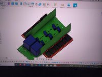
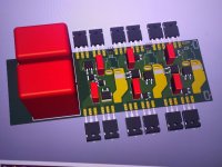
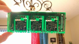
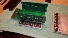
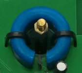
I started talking with Shaman a while ago about power stage design. Talking about this stuff motivated me to design a power stage which has 12 to 24 TO-247/TO-264 MOSFETs / IGBTs to test out some design ideas I thought up. I'm still using the TD350E gate driver chip for now because I know it works really well, is isolated and I've built multiple gate drivers with it into the 300A range. I'm planning to swap to something a bit newer in the near future, but qualifying a new gate driver takes some time. This setup can do about 50kHz max which is more than most motors need. DC link caps are 500V 90uF 26A ripple each, so running low inductance motors should be possible. Screw lugs accept up to 2AWG wire and I put dual feeds on the DC side. If I scale up to 18 or 24 FETs I'll add dual to the output and run 3 on the input, I'd also add more caps. The MOSFET legs are surface mounted to the PCB, so it pretty much eliminates the leg current limits and the PCB helps dissipate the heat from the legs. This also keeps the gate driver components cooler as the only thermal interface is the small PCB holes the legs go through. I can also swap out for TO-220 devices and run a bunch of them in a 24-36FET setup. Current sensors are Allegro 200A units, but I've also included a bypass shunt option which allows me to increase the sensor range from 200A all the way to 400A easily. This saves cost on current sensors.

I'm attempting to use a PCB as the DC bus. I've performed many CFD analysis simulations and it looks quite doable with 6 layer PCBs depending on manufacturing cost (it looks doable but I don't have an official quote). I've been bench testing a 6 layer PCB with 2oz top / bottom and 0.5oz inner layers and it will do 40A DC but is limited with the phase output (2.5oz) as the traces are not as wide. I put 40A DC through it and leaving it on for an hour, thermal run away started at ~45A in a 25C room. Production would be 4oz on all layers.

A benefit with the 6 layer PCB is my DC bus can be put on alternating layers which assists in lowering the inductance. I've measured this design at just under 20nH. I've also added an optional clamping RCD snubber which recovers ~50% of the energy it absorbs back into the DC bus, so far it doesn't look like I'll need it. I've been putting ~600A pulses through 2 parallel MOSFETs and turn off overshoot is <10V over bus at 62V, this will probably drop even more >100V bus. I could also swap in IGBTs and go to higher voltage.

It also has an improved thermal path on the MOSFETs as I've been able to eliminate the insulator directly underneath the MOSFETs. In near ideal conditions a 5mOhm TO-247 can sustain 100A DC at 25C ambient with forced air cooling for 3mins with a case temp < 80C. This means much higher short current bursts can be achieved, probably 180-200A peak per device for at least 10s, just speculating. So far current sharing between devices is looking good and I didn't even RDSon match them as I did in past projects.

I'm planning on using a 3D printed case with built in duct work for air cooling the PCB and gate drivers.

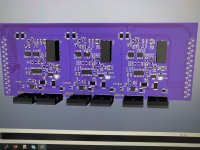
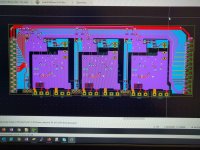
In order to test the power stage out I needed a controller, so I decided to go the VESC route. I designed up some PCBs similar in design to what Axiom has done. I didn't use a FPGA though, instead I used discrete logic to provide hardware fault detection, indication and shut down. I went a bit overboard, but it was a fun exercise to improve my logic gate skills. It mostly works, just doesn't reset correctly, got a bug somewhere. Has all the same hardware based fault detection, over current per phase, over voltage per phase / DC bus. Just go look at the Axiom schematic to get an idea, then imagine a version of it that is a few notches down to save cost and not worry about automotive certified parts.

I'm about to start the VESC journey, I heard it is an interesting and often frustrating one so that I can hook this up to my dyno and see how it runs under real world load.

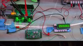
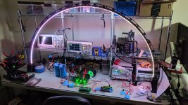
I have more videos and pictures I'll post up later, right now here is one showing the power stage/gate driver. The lower boards (triple stack) are the VESC controller and the thing with the LCD is my double pulse tester.

Short video of me shorting the output to simulate shoot through to see if the MOSFETs would blow up (they never have on this gate driver).
https://youtu.be/bvqAEGtAvEM

Before anyone says something about the PCBs needing support, they have it, it's built into the case which isn't shown here.

If anyone is interested in a power stage like this let me know. When I get bored I like to engineer stuff, now if only I can find people that want to buy it. Designing it is the easy part.
 

Attachments

  • Workbench-Pulse-testing.jpg
    Workbench-Pulse-testing.jpg
    178.5 KB · Views: 5,225
  • Workbench.jpg
    Workbench.jpg
    215.1 KB · Views: 5,208
  • Concept1.jpg
    Concept1.jpg
    80.1 KB · Views: 5,213
  • Concept2.jpg
    Concept2.jpg
    109.1 KB · Views: 5,213
  • PCB Gate Drive.jpg
    PCB Gate Drive.jpg
    150.3 KB · Views: 5,214
  • PCB grounds.jpg
    PCB grounds.jpg
    174.1 KB · Views: 5,207
  • Gate Driver.jpg
    Gate Driver.jpg
    181.4 KB · Views: 5,207
  • VESC.jpg
    VESC.jpg
    212.5 KB · Views: 5,222
  • Prototype.jpg
    Prototype.jpg
    276.2 KB · Views: 5,223
Nice job , I love your LED stargate. I could be interested in the gate driver boards for a 24 fet TO-247 setup. I think for a 24 fet setup 400 amp current sensors would be insufficient. I am going to give the Melexis MLX91205 sensors a try since they are not badly priced and good for up to 800 amps clamped to a phase lead/bus bar. I have found the IRFP4568's good for 150 peak phase amps on Lebowski's last 6 Fet power power board so I am aiming for 600 amps with a 24 fet design.
 
kiwifiat said:
Nice job , I love your LED stargate. I could be interested in the gate driver boards for a 24 fet TO-247 setup. I think for a 24 fet setup 400 amp current sensors would be insufficient. I am going to give the Melexis MLX91205 sensors a try since they are not badly priced and good for up to 800 amps clamped to a phase lead/bus bar. I have found the IRFP4568's good for 150 peak phase amps on Lebowski's last 6 Fet power power board so I am aiming for 600 amps with a 24 fet design.

Part of this is experimentation and that includes running higher current on the current sensors by shunting them as I have not done that with these sensors. In the past I've used HASS sensor for higher current stuff, but they get more costly. I haven't worked with the Melexis style sensors yet, but I have read up on them a little. I decided to go with stuff I know works for this design and get more experimental later. Downside to bigger current sensors is less resolution which can sometimes be an issue.

I'm currently using IRFP4568's on this 1st prototype for initial testing since I had a bunch of them and am familiar with their switching characteristics. The next one will have IRF200P222s. What was the thermal interface between your devices and your heat sink on the 6 FET and how long were you holding 150A phase?
 
zombiess said:
DC link caps are 500V 90uF 26A ripple each
Any reason you chose two large caps over multiple smaller caps? Nice choice moving all the way up to the DC link PP film caps.

zombiess said:
I'm attempting to use a PCB as the DC bus.
Looks like you've more than attempted it! Throw enough layers of heavy copper at it and it should be fine. Soldering the components will be less fun if you're doing the assembly.

zombiess said:
It also has an improved thermal path on the MOSFETs as I've been able to eliminate the insulator directly underneath the MOSFETs.
How are all 6 of the low side FET drain terminals directly connected to the same heat spreader plate without being isolated?

zombiess said:
If anyone is interested in a power stage like this let me know
I am interested but would have nothing to use it with! Nice work on it though. You've added to the already copious amount of good reading regarding controllers.
 
I'll buy two 200A 200V controllers please. I need to take back the top speed with a hubbie record that Rovi stole with a motor that fried in a few runs vs mine on a daily rider since 2012.
 
Hi,
First, kudos on that great work, seems well done!

I'm not sure to understand what's going on there exactly: that's a power stage that is separated from the actual brains, meaning you can plug any kind of brain you want to control the gate drivers, which, by extension, control the mosfets?

Something I'd like to do for years is to replace the power stage of a Sabvoton controller. I really like these controllers but the only thing I'd like would be to get a bit (well, a lot) more power from it. So the idea I hope to achieve someday is to remove all its power stage and build a separate, much more powerful one in an other bo next to it.
Currently it is set up at 210A battery, 510A phase, I'd like to go as high as possible, my battery could deliver 600Amps and I'd be open to change my motor to be able to reach 1200A/phase if it comes to that.

Sorry if my question is foolish to you, but would that be feasible in your opinion?
Could your design scale up to that kind of power?
 
Dui said:
I'm not sure to understand what's going on there exactly: that's a power stage that is separated from the actual brains, meaning you can plug any kind of brain you want to control the gate drivers, which, by extension, control the mosfets?

My goal is to build a reliable standalone power stage with gate drivers and needed sensors that other designers could utilize in their own projects. Designing a good power stage and gate drive is a non trivial task.

I have other prototypes which are capable of much higher currents, but they are still in development, however initial prototyping has shown near equal current sharing with 9 TO-247 in parallel. I still need a more appropriate gate driver (and current measuement technique) for that power level.

The VESC controller is just something i built to help me test this power stage by running a motor. I have a two older Montenergy me-0913 motors setup as a dyno i eventually want to use for load testing this design.
 
bww129 said:
Any reason you chose two large caps over multiple smaller caps? Nice choice moving all the way up to the DC link PP film caps.

I went with the most cost effective solution for high ripple current handling. I'm a fan of PP caps as they provided extremely long life and high ripple current handling. I can add on more caps if needed, but the load inductance and switching frequency determine the sizing of the DC link caps. These caps are small compared to the ones on my other project which will use 3 PP caps, each rated for 100A RMS ripple each.

Looks like you've more than attempted it! Throw enough layers of heavy copper at it and it should be fine. Soldering the components will be less fun if you're doing the assembly.

Soldering is a non issue with a properly sized iron and I have some ginormous soldering irons commonly used for stained glass work.

How are all 6 of the low side FET drain terminals directly connected to the same heat spreader plate without being isolated?

Insulators go between the pucks and the spreader plate. The pucks provide thermal mass and larger surface area to transfer heat into the spreader plate. I'm trying to measure the difference in thermal resistance today.
 
zombiess said:
Part of this is experimentation and that includes running higher current on the current sensors by shunting them as I have not done that with these sensors. In the past I've used HASS sensor for higher current stuff, but they get more costly. I haven't worked with the Melexis style sensors yet, but I have read up on them a little. I decided to go with stuff I know works for this design and get more experimental later. Downside to bigger current sensors is less resolution which can sometimes be an issue.

I'm currently using IRFP4568's on this 1st prototype for initial testing since I had a bunch of them and am familiar with their switching characteristics. The next one will have IRF200P222s. What was the thermal interface between your devices and your heat sink on the 6 FET and how long were you holding 150A phase?

The 4568's are screwed to a 1/4" piece of aluminum angle with mica insulators which is in turn screwed to an aluminum case. Peak phase amps wouldn't be for more than a few seconds at a time during a normal drive cycle because the motor accelerates pretty quick.

I will very interested to see your current sensor shunt arrangement, it would be great to get 400A capability out of a 200A Allegro sensor. A guy over on openinverter rolled his own current sensors using SS49E's and Epcos B64290L0618X035 ferrite core. You can tune the sensitivity by changing the gap size. I took a close look at the Honda IMA inverter current sensors and they a built on the same principle. DIY Current sensor.PNG
 
zombiess said:
My goal is to build a reliable standalone power stage with gate drivers and needed sensors that other designers could utilize in their own projects. Designing a good power stage and gate drive is a non trivial task.

Yes, that's a big reason I ended up using the Honda IMA inverter as a powerstage for the Lebowski brain (a project I still have to finish and test); was the least expensive way to get what I needed...but it's on the huge side for the power levels I need. :oops:
 
For those wondering about the pucks which are in direct contact with the MOSFETs, here is some data which explains why I am using them.

I used an IRFP4668 MOSFET for the following tests which has an RDSon of ~9mOhm and supplied the gate with +15V and used it as a heating element on an old all copper Xeon CPU heat sink with a high flow fan. The case temperature was read with a K-type thermocouple and I ran the setup until a steady state case temp of 70C was reached, after 80C things go into thermal runaway VERY quickly. Voltage was read kelvin style at the drain and source legs right at the entrance to the MOSFET body.

I think the Kapton tape was 0.003" thick

The best case scenario is:

Heat sink -> Thermal Grease -> Mosfet
This resulted in 74A DC with a voltage of 1.24V resulting in 92W of heat produced @ 70C case temp.

Heat sink -> Kapton Tape -> Thermal Grease -> Mosfet
This resulted in 39A DC with a voltage of 0.63V resulting in 25W of heat produced @ 70C case temp.

Heat sink -> Kapton Tape -> Thermal Grease -> Aluminum Puck -> Thermal Grease -> Mosfet
This resulted in 55A DC with a voltage of 0.84V resulting in 46W of heat produced @ 70C case temp.

Heat sink -> Kapton Tape -> Kapton Tape -> Thermal Grease -> Aluminum Puck -> Thermal Grease -> Mosfet
This resulted in 54A DC with a voltage of 0.95V resulting in 51W of heat produced @ 70C case temp.

Heat sink -> Silicone Pad -> Mosfet
This resulted in 35A DC with a voltage of 0.61V resulting in 21W of heat produced @ 70C case temp.

The silicone pad really surprised me, I did not expect it to perform as well as the tape due to how much thicker it is.

As can be seen from the data, using and insulator between the puck instead of using the insulator between the MOSFET and the heat sink increases the power handling capability of the MOSFET by 2x and allows for about 40% more current. The larger the puck, the bigger the gain. The pucks are attached to the base plate with 4 nylon screws to avoid causing any shorts. I've never had an issue using Nylon screws in applications < 100C.

The IRF200P222 MOSFETs have a 6mOhm RDSon, so even higher current is possible with them. 150V and 100V parts have even lower RDSon to allow for higher current if higher bus voltage is not required, however getting the desaturation protection to work becomes a bit trickier as RDSon drops.

I also ran tests in the different configuration on how long it took to go from 30C to 65C once I found where the steady state current was. The answer is 2.5 to 3 mins.
 
Great work Jeremy,

Good to see you still at this. Just push forward and see what happens!
 
Thanks for sharing, I've learned a great deal reading your posts about inverter and gate driver design, and I'm hoping to try out what I've learned from you for myself in the near future. It's really cool to see your bus and thermal layout considerations, and a great learning experience for a baby EE myself. If I'm understanding properly, is your stackup on the 6 layer power PCB Bus+, Bus-, Bus+, Bus-, Phase, Phase/Snubbers? Does the extra pair of layers halve the inductance in the power stage?
 
I was curious what the junction temps of your tests were, so I did my best to back them out of the datasheet and your numbers. Figured I'd share since I'd already done the work. Based on your comments about runaway, they're unsurprisingly above 100C. The numbers for the single layer of kapton and aluminum puck are suprising though - perhaps you could run a slightly higher case temp, not that its necessary. I was assuming a nominal Rds of 8 mOhms.

7JpDmPL.png
 
SRFirefox said:
I was curious what the junction temps of your tests were, so I did my best to back them out of the datasheet and your numbers. Figured I'd share since I'd already done the work. Based on your comments about runaway, they're unsurprisingly above 100C. The numbers for the single layer of kapton and aluminum puck are suprising though - perhaps you could run a slightly higher case temp, not that its necessary. I was assuming a nominal Rds of 8 mOhms.

7JpDmPL.png

That single layer + puck is most likely a bit of an outlier or I goofed on my measurement, but it's in the ballpark. Previous experience in thermal test has shown as little as a 1A increase could push it from 75C to 80C in a few seconds and then 80C to 100C in about 2s. It behaves like a flash over point, so I aim to keep the case temperatures < 75C as there is also a lag in the response. 70C provides some reaction time to throttle back the current.

Your junction temps are about what I came up with as well. General safety margin rule with electronics is to not exceed 80% of an absolute max, so with a max 150C junction temp, 120C is the magic number to stay below.
 
SRFirefox said:
If I'm understanding properly, is your stackup on the 6 layer power PCB Bus+, Bus-, Bus+, Bus-, Phase, Phase/Snubbers? Does the extra pair of layers halve the inductance in the power stage?

The layer stackup you posted is about correct. I could have gone + + - - P P, but there loop area would be a bit larger. The inductance is related to the loop area. Alternating + - + - P P produces a loop area which is a bit smaller and therefore cancels out more of the induced EMF. This results in a lower inductance on the DC Bus. When building a DC bus you want the + - to be as physically close as is possible/safe. This reduces turn off overshoot, reduces the amount of snubber needed and gives you additional voltage headroom.
 
This is really cool. I like the PCB laminated bus and heat dissipation puck ideas. It looks like the puck is around (120C-25C)/51W=1.86 C/W Rtheta junction to ambient/isolated heatsink which are pretty much the same thing in this setup.

How are you transferring current between layers on the PCB? You mentioned surface mounting the mosfet legs, but it also looks like there are through holes for the legs on the pads as well?

Have you thought about testing copper pucks? With almost double the thermal conductivity, the extra cost might be worth it. You could also maybe solder the TO247 tab to the copper instead of screwing it down with thermal grease.

I've also seen IMS PCBs used as the insulator instead of kapton. Another option to consider...
 
thepronghorn said:
This is really cool. I like the PCB laminated bus and heat dissipation puck ideas. It looks like the puck is around (120C-25C)/51W=1.86 C/W Rtheta junction to ambient/isolated heatsink which are pretty much the same thing in this setup.

How are you transferring current between layers on the PCB? You mentioned surface mounting the mosfet legs, but it also looks like there are through holes for the legs on the pads as well?

Have you thought about testing copper pucks? With almost double the thermal conductivity, the extra cost might be worth it. You could also maybe solder the TO247 tab to the copper instead of screwing it down with thermal grease.

I've also seen IMS PCBs used as the insulator instead of kapton. Another option to consider...

Copper is too costly, but I have done some designs (untested) where the TO-247 package is soldered to a copper backing plate. I know this is doable as I have an example, however if I want to offer this for sale, it's another fabrication step which would likely yield little benefit. I've also simulated the electrical and thermal properties of aluminum vs copper bus bars in CFD and found that copper only provided a small advantage. I've also had an experience bus bar designer tell me copper would likely not show much gains in my application.

The current is transferred with vias surrounding all high current transfer points. The holes where the MOSFET legs mount are acting as both vias and mounting holes. I decided to provide myself with the option of not using the pucks if they add too much cost, but in that case, the legs would need to be placed through hole or bent into a step shape. This is needed for additional clearance between the PCB and the heat spreader plate. I have D2Pak diodes and resistors mounted on the bottom side of the board if I need to install the RCD snubber components.

I just realized that I had forgotten to run a test without any insulators with just the thermal grease so that I could see how the best puck setup (but no electrical isolation) compares against the optimum solution with insulation.

When I made this test the ambient room temp was 5C lower than last time, so these results are probably a little better. I haven't noticed the ambient temp producing any note worthy difference on heat sink temperatures or current handling capacity of the devices. Probably because the heat sink is way over sized + extreme forced air cooling.

Heat sink -> Thermal Grease -> Aluminum Puck -> Thermal Grease -> MOSFET
This resulted in 65A DC with a voltage of 1.01V resulting in 65W of heat produced @ 70C case temp.

So the no isolation no puck setup is:
(120C-25C)/92W = 1.0 C/W

The no isolation with puck setup is
(120C-25C)/65 = 1.5 C/W

Add on some kapton for electrical isolation between the puck and sink
(120C-25C)/50W=1.9 C/W

This means the kapton + thermal grease adds 0.4 C/W, not bad, not great, but low cost.

The pucks provide a 2x improvement vs mounting directly to the kapton.
(120C-25C)/25W = 3.8 C/W of the:
Heat sink -> Kapton -> Thermal Grease -> MOSFET

Getting 2x the power handling by simply adding the puck is a huge jump power handling for very little cost. I can also increase the length of the puck to gain more improvement as I have done with the TO-264 design.

This design is empirically verifying some design concepts I've come up with which I'll be using in my own custom, very high current (+1kA) modules.

I should be much further along, but working on this kind of stuff solo causes me to lose some motivation after a few months. Finding other motivated designers to team up with is challenging, no one has the time and even fewer have experience in power electronics.
 
Try flat heatpipes between mosfets and heatsink. I've used those in couple of custom high power LED lights, the heat transfer is amazing.
Mounting will be more difficult - basically; either clamping + thermal grease or just thermal epoxy.
 
Nice design, congrats! Great info on thermal tests, too, but I'm wondering something:
In the datasheet the junction to case thermal resistance is 0.29 C/W. As in all test configs the case temp was 70C, then the junction temp would be different:
first case: 70C + 92W*0.29C/W = 96.68C
last case: 70C + 21W*0.29C/W = 76.09C
I assume you measured the case temp on the plastic part of the package that must be cooler than the metal base of the FET. Then from the other direction, from the Tj-s calculated by SRFirefox the case temp (metal base):
first case: 116.05C - 92W*0.29C/W = 89.37C
last case: 121.43C - 21W*0.29C/W = 115.34C
These are quite hotter than the 70C, especially the last case, can you explain that? Is this difference between the metal base and the plastic realistic?
 
minimum said:
Try flat heatpipes between mosfets and heatsink.

More complicated and costly vs having a CNC machine spit out pucks made from off the shelf bar stock.

peters said:
Nice design, congrats! Great info on thermal tests, too, but I'm wondering something:
In the datasheet the junction to case thermal resistance is 0.29 C/W. As in all test configs the case temp was 70C, then the junction temp would be different:
first case: 70C + 92W*0.29C/W = 96.68C
last case: 70C + 21W*0.29C/W = 76.09C
I assume you measured the case temp on the plastic part of the package that must be cooler than the metal base of the FET. Then from the other direction, from the Tj-s calculated by SRFirefox the case temp (metal base):
first case: 116.05C - 92W*0.29C/W = 89.37C
last case: 121.43C - 21W*0.29C/W = 115.34C
These are quite hotter than the 70C, especially the last case, can you explain that? Is this difference between the metal base and the plastic realistic?

You are correct that I am measuring the temperature on the plastic MOSFET case, not the tab. The reason I'm measuring at this location is it runs hotter than the heat sink itself and gets up to temp very quickly. The hottest part of the MOSFET is right by the source leg on the case as can be seen in this video I made using FLIR:
https://youtu.be/qu6Q-RHhHXk

The bond wires from junction to source leg are the hottest part on every MOSFET I've tested.

For my own measurement purposes I decided to place the probe in the center of the plastic case as that is where I intend to measure for any thermal throttling/shut down.

I never trust datasheet ratings for current/thermal ratings as they are unobtainable in real use scenarios, but can be good for comparing one device to another with enough experience. Same goes with CFD simulation, it's good for figuring out design changes, but it's not reality, just an approximation to compare design ideas under similar physics. It doesn't need to be accurate to be useful, it just needs to be consistent in approximating reality.

I'm applying the same concepts I learned from dyno tuning 100's of ICE engines. The dyno "horsepower" number should only be used to determine if the tuning change/part had a desirable effect, not to measure actual "horsepower".

I know from bench testing on my test apparatus that thermal runaway accelerates rapidly at around 80C at my measurement point with a very small increase in current on every device I've tested, both TO-220, TO-247 and TO-264 with various RDSon values.

As for why the math isn't working out, I don't have a solid answer for you other than my testing conditions are not the same as the ones used for the datasheet.

Testing methodology:
http://www.irf.com/technical-info/appnotes/an-1140.pdf

Section 8 on how to determine the maximum current handling capability of a device has some great comedy in it:

Measure TL and Tb vs current. Take several measurements over different currents. Record the current and the temperature of the lead and solder attach point. Allow the system to sit for at least 3 minutes at each current level. If the soldered-on thermocouple falls off, then that is a good indication that there is too much current.

I love engineering humor.
 
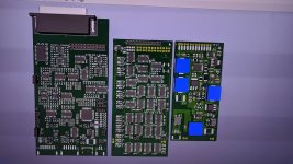
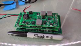
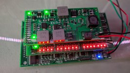
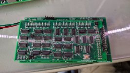
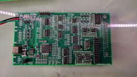
This is the VESC based controller I'm working on to control the power stage. It's based off the Axiom schematic with modifications made for my needs.

It was an interesting experience doing all my fault handling in discrete logic gates and flip flops. Usually I use a micro-processor like a PIC or Arduino to handle faults, but I wanted to use hardware based fault detection for increased safety.

Levels of protection:
The power stage has desaturation detection setup for use with my MOSFETs to detect shoot through and shut down the gate drive, this also signals a fault condition to the fault logic board, which then shuts off PWM to the gate drive, the fault signal also triggers a fault on the controller causing it to stop sending PWM as well. Over voltage, over current is detected on each phase, over voltage on the DC bus and over temp conditions for MOSFET/PCB/other analog inputs are all done by hardware shutdown.

Took three 4 layer boards to fit in all these features in a size that would work for my project.
 

Attachments

  • VESC-01.jpg
    VESC-01.jpg
    178.9 KB · Views: 4,381
  • VESC-02.jpg
    VESC-02.jpg
    195.8 KB · Views: 4,382
  • VESC-FaultLogic.jpg
    VESC-FaultLogic.jpg
    224.8 KB · Views: 4,382
  • VESC-MainBoard.jpg
    VESC-MainBoard.jpg
    248.6 KB · Views: 4,382
[youtube]IiSUx-ryoD0[/youtube]

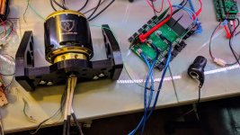
It took about a week of hardware and software debugging, but I finally got my VESC controller and power stage to spin a motor in FOC mode. Shaman was a big help in providing pointers on the VESC setup. Unfortunately VESC does not appear to have much documentation on how to setup your own hardware. Axiom's files came in handy by allowing me to make comparisons to their .h and .c files vs normal VESC hardware configs which eventually allowed me to figure it out. I think the previous work I've done on TI's Instaspin motor drive prepared me well for doing battle with VESC as it too has poor documentation. It's all about getting in and trying to understand the code.

For my test motor I'm using a 1000KV 2212 size RC motor. The 200A current sensors don't seem to have issues running it. I plan on adding shunts to turn the 200A sensors into 300A and 400A sensors to see how far I can push them. As is everything but the MOSFETs are configured to operate up to 200V. The voltage readings are scaled for a max reading of 220V. It's a lot of controller for this little motor.
 
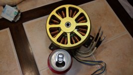
I managed to get this beast running tonight without much issue in FOC. It's a controller killer at 8uH inductance phase to phase on 4gauge leads. 70KV. I cant rally load it for more testing, but i wanted to see if it would work. The only setup I have which I can load uses 2 older Montenergy ME-0901s, so it's not very lab friendly, but I'll have to figure that out.

I'll try to grab some video of it running tomorrow. The VESC software is only measuring the inductance at 1/3rd of actual on my meter. I need to look at the code and try some different motors. Maybe I can mod the code to be more accurate for the PI controller gain calcs.
 

Attachments

  • IMG_20200706_222646_copy_1608x904.jpg
    IMG_20200706_222646_copy_1608x904.jpg
    207.3 KB · Views: 4,120
  • IMG_20200703_193203_copy_1344x756.jpg
    IMG_20200703_193203_copy_1344x756.jpg
    132.7 KB · Views: 4,120
Back
Top