Arlo's power stage Leaf controller runs and drives page 103

HighHopes said:
that looks really good arlo, appreciate sharing the pictures.

i can help you exactly with correlating junction temperature with switching frequency using mathematics. unless you are asking about bench testing, i have never used that mosfet before so can not say. will this math help you ?

you will be hard pressed to get 300A through 4 parallel mosfets. the case lead is limited to 75A, and that is under ideal conditions with DC current. 4 in parallel is 300A... there is no derating here, but there should be. in fact, there MUST be, even if you match the mosfets (just less deratinng if you match).

good luck!!!
Thanks HighHopes.
Any data for switching time changes for any fet you can give the better. Even some numbers from other types of fets to use as rules of thumb will help estimate how much extra of a buffer I should add to the dead time to make sure it will last.

I was reliable with 250 amps with 3 in parallel of the same package size and a poor layout. I think I can make 350 phase amps reliably. But you are the one who really knows.
I do agree with de-rating. This is motor(phase amps) and its not really DC... they work for 2/3 the time the controller is running... Well I think lebowski's code might work a little different but the theory is 2/3 the time and from there its in a PWM fashion with the amps flowing in a sine wave so it might be 350 phase amps peak but not a average....
 
Wow!!! That is very beautiful work Arlo! Woot! I need to mail you something to power with it. :)
 
Thanks guys. I run some tests with 8s lipo on the bussbar and I was getting some bad ringing but switching the gate resistors up to 43ohm made it go away then back to 30 ohm is pretty good but with a touch of ringing and only 3v over shoot. I know I should run the voltage I plan to run for this but I got to get it close before going up to that voltage. I set this up for a few options for adding diodes/resistors in series/parallel. I think I will run a 2 or 3 ohm resistor in series with maybe a 20 ohm resistor.
Right now the testing I have done is with just 1 resistor per FET so 4 resistors I have the option to add a single resistor and or diode in series with all 4 fet resistors if I want but right now its just got a jumper. I remember Shane Colton recommending most of the resistance to be in the 1 main resistor and a small resistance per fet closer to the fet. What do you guys recommend?

As for the dead time numbers
10 ohms per fet give me .03 amps at 166ns dead time
30 ohms per fet give me .03 amps at 600ns dead time
43 ohms par fet give me .03 amps at 900ns dead time
in all cases lower dead time caused the amps to increase. This is where calculations or even a rule of thumb comes in sure it will run ok cold at this dead time but when it heats up the dead time should be higher.... I think. So maybe 50% more? IE 900 ns with a 30 ohm gate resistor per fet?
 
For stopping FET ringing, better than just applying R alone, throw a ferrite bead around the gate leg. When the system tries to self-resonate between the miller plateau voltage just being reached on the gate, and the ferrite's coil collapses as the induced source voltage starts to lift from it beginning to conduct. That field collapse in the ferrite is just enough to keep the current moving in the right direction continue saturating that gate charge rather than flutter and make the spikes you're seeing.

As you know of course, this ringing grows directly with current typically, so if you want to go big and keep it alive, your ringing should be as close to zero as possible.
 
Thanks I tried the ferrite bead thing before with little luck. The bead goes on the fet gate leg right? Can it go further up the line ie. On one end of the gate resistor? I don't feel like unsoldering the FETs to try at this point.
On the ringing end I found current was causing ringing that was not able to be controlled by anything other than layout and caps and diodes on then rails. The. Test so far is unloaded in pwm test mode BTW.
 
Arlo1 said:
Thanks I tried the ferrite bead thing before with little luck. The bead goes on the fet gate leg right? Can it go further up the line ie. On one end of the gate resistor? I don't feel like unsoldering the FETs to try at this point.
On the ringing end I found current was causing ringing that was not able to be controlled by anything other than layout and caps and diodes on then rails. The. Test so far is unloaded in pwm test mode BTW.


Should work fine on the resistor leg near it. If 1 doesn't work, add them until it does. (or at least give it a shot)
 
as dead time increases, the AC output voltage distortion increases and is no longer sinusoidally shaped perfect.. so the peak is not there any more and so the current decreases. as a rule of thumb, your dead time to switching period ratio should not exceed 5%, otherwise way too much distortion and your system suffers to a point where a new design would be better... or ask Lewbowski about his deadtime compensation software version.

dead time works like this. it is always safe to turn a mosfet OFF instantly.. but it is not necessarily safe to turn a mosfet ON. if you want to turn a mosfet ON you must be absolutely SURE that the other adjacent mosfet is OFF. since your gate driver makes no measured determination of when it is actually off, you have to guess.. i.e. by applying an arbitrary delay of fixed duration, "deadtime", weither or not that time was way too much or just enough.. always the same value, not dynamic.

we can make an educated guess at what an appropriate worse case dead time should be. to do this you must be able to understand where all your signal propegation delays are. i.e. i want to turn Mosfet OFF but i know this does not happen instantly. how long does it take for this OFF signal to leave the digital controller and actually see a mosfet drain/source voltage increase to DC bus voltage? where are the major delays? digital to gate driver is negligable. at input of gate driver is usually some sort of isolation (i don't know your design, have not seen schematic) and this isolation, like an opto-coupler, usually has some delay time. if you are using an IRF gate driver chip then read the datasheet to see what its MAXIMUM propegation time is to turn a mosfet OFF. the next delay will be in the boost stage if you have one. the next is in the mosfet fall time (see datasheet). the final is fall time delay of mosfet (also see datasheet). look for maximum values (worse casae). if the max is not listed, only typical, then you have to calculate the fall time & delay by reading the curves of the datasheet. i can help you more here if you need it. take this total propegation delay time and that is your dead time. i realize that the ON command of mosfet also has delay, theoretically the fastest time this can turn on could be subtracted from the previous calculation to get a more fine tuned dead time but i don't do this, i like to ignore the turn ON time factor and think of it as added safety margin. now check that deadtime with respect to your switching period.. less than 5% good. greater than 5%? lower your switching frequency or change your gate driver design or mosfet selection.

gate resistors.. having one or two low resistance and then a third as 20 ohms just means that the 20 ohm resistor will take the bulk of the power losses and should be sized such. to me it does not make any sense at all to do it this way, the resistors should all be same value. only time you would have values significanly different is if you had one resistor (or group of series resistors) driving ALL parallel mosfets and then a second single gate resistor of much lower value PER mosfet.

that is 20 ohm each per parallel mosfet? that is huge... look at your mosfet datasheet and find the curve that describes switching time vs. gate resistance. on the X-axis will be gate resistor.. if your total series gate resistance is greater than the highest value on that X-axis then it is too high and your mosfet will underperform (switching times too long for mosfet die level design). so you will have higher than necessary swithcing losses and stress mosfet due to length of time in linear region. if this becomes a problem solution is to lower gate resistor or if you can not (due to some not ideal problem in system design) then lower the switching frequency. lowering temperature will have little effect here as this has little to do with mosfet switching losses.

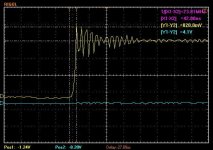
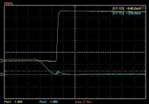
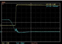
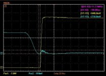
#1 cause of ringing is power bridge assembly.. clean layout, laminated bus bar, quality parts.
always some ringing is normal. typical thing to do is increase gate resistance until you can find a balance between decreased ringing and mosfet power dissipation. you can only increase the gate resistance so far though (see further below).

another, less likely, cause is:
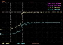
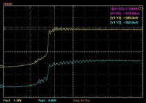
one thing about your design is that your mosfet heatsink also carries phase current. that is unusual.. never seen that before. not too big a deal in of itself, but this phase output heatsink also has a switching voltage on it. your chassis will have some other voltage, probably 0V. between the two is a piece of kapton tape. so this is like a capacitor.. two plates of different potential with a dielectric between them, ya? and the plates are large area just like capacitors appreciate. on top of that is one of the plates not only has a potential, but it is a changing potential.. from bus voltage to zero, and repeat 40,000 times a second. this will inject a current.. i = C*dv/dt. if this capacitor were to be of such a value as to resonate with an inductance that is elsewhere in the network that would cause ringing. the mosfet switching goes through a HUGE frequency spectrum so it is quite likely to find a resonance if there is such an LC network..

i would need to know more about your design in order to help with the ringing issue. or you can try solving by trial and error different tests.

for Mosfet switching losses & junction temperature my preferred reference is "MOSFET Power Losses Calculation Using the Data-Sheet Parameters" by infineon. all the manufacturers have their own formula for mosfet switching losses .. unfortuantely. it is not like IGBT where datasheet gives switching losses in convenient single unit of joule. no.. for mosfet it is all timing waveform extrapolation and so weird formula :( i have worked out fully the math for this if you want but it is basically just the infineon app note with some modifications i made. i do not linearize the mosfet performance as infineon suggests, instead i take the datasheet curve as it is, with a shape.. not a straight line and curve fit. linearizing is OK if your operation never changes.. like a DC/DC converter with a fixed load. but a sinusoidal current output goes through 0amps to max amps in ONE cycle! and it changes all the time depending how the driver presses the gas peddle.. also, for junction temperature it is important to iterate which infineon does not do. that is, use their app note to calculate the power dissipation (but use curve fit technique instead of linearization) then calculate what the junction temperature will be. then, with that new junction temperature.. re-calculate the power dissipation, and repeat until successive iterations have less than 2 degC between them. then your result is much more accurate & now actually useful for power bridge sizing.

$0.02
 
HighHopes said:
that is 20 ohm each per parallel mosfet? that is huge... look at your mosfet datasheet and find the curve that describes switching time vs. gate resistance.
Thanks for all the info I will do some more testing...
I have a Curtis Brushed DC controller with 47 ohm gate resistors..... I know I want to keep the switching as fast as possible with little ringing as possible so I will try Lukes suggestion first then see what I can come up with.
I will get it as good as I can before running loaded tests on the dyno with a motor.
But I could not find this....

http://www.irf.com/product-info/datasheets/data/irfp4568pbf.pdf
 
Wow Luke the ferrite bead is working this time but... It slowed the switch down from around 500ns to 1us. I will drop the gate resistor value and see what it looks like scope screen shots to come :) Man I love this shit! :)
 
Arlo1 said:
Wow Luke the ferrite bead is working this time but... It slowed the switch down from around 500ns to 1us. I will drop the gate resistor value and see what it looks like scope screen shots to come :) Man I love this shit! :)

Right on. :)
I'm stoaked for you. That was a Bigmoose taught trick. :)

You don't have to ring. It can be tuned out, and IMHO its worth the tuning.
 
Ok here is the last two screen shots before bed. I run a bead in series with all the fet gates. So I went all the way down to a 10 ohm resistor per gate and the bead then the next test was a 1 ohm resistor with a diode in parallel for faster off time followed by the 1 bead then from there the 4 separate 10 ohm gate resistors this looks a little better and I think its going to be ok its less then 2v over shoot! At 500ns dead time the amps are as low as they can go so I set it to 700ns for now then I will re test in the future. Yellow is drain-source on the low side and the blue is the high side gate. (just sorting one side out first) The voltage scale is off by 10x because the program doesn't know I had the probes on the 10x setting. And from the time the gate starts to move the smallest bit to the drain is full on is <500 ns which is decent switching times for this fet. My last working controller was >1us switching times and it worked ok up to 20khz.
 

Attachments

  • 10 ohm with bead only.JPG
    10 ohm with bead only.JPG
    54.1 KB · Views: 2,334
  • Capture.JPG
    Capture.JPG
    55.9 KB · Views: 2,334
Here is a screen shot of the drain to source on the low side with just 10 ohm gate resistors this is where I started.
The only ferrite beads I could find in stock are... Bead core 3.5mm axial PN P9820BK-ND http://www.digikey.ca/product-detail/en/EXC-ELSA35/P9820BK-ND/44717
Repeat this is before I fixed the problem with Luke's suggestion.
 

Attachments

  • 10 ohm gate.JPG
    10 ohm gate.JPG
    53.9 KB · Views: 2,313
1us switching time is excessive. not necessarily a bad thing, just means that you will dissipate far more losses in switching than manufacturer intended. easy enough to compensate for.. lower the switching frequency. use a laser temperature sensor to watch your mosfets (each one) during some long operation testing and get a sense of what your case temperature is. 70-80deg C is max for case temperature.

not sure how much time you want to spend development testing, but it can be worth your while to determine what the cause is of the ringing and solve that instead. or add inductor and lower switching frequency and move on.

keep it up, you are an inspiration for grit & determination
 
Highhopes my switching time is < 500ns. I was comparing to the last design with a pour layout. I'm already working on a new version of these boards to reduce the fet driver inductance. So judging from the pictures would you clean up the ringingn a little more?
 
Ok, a new shinny one Arlo :). Here we go again closely following your endeavors :)

HighHopes, what do you think about the approximation formula below for MOSFET switching dissipation?

Pd(sw) = 1/2 . Vd . Id . (tr + tf) . fsw

Pd(sw) - Power dissipation when switching
Vd - Top drain voltage (or just "system Vcc")
Id - Top drain current
tr, tf - Switch on and off times (time spent in the linear region)
fsw - Switching frequency
 
HighHopes, what do you think about the approximation formula below for MOSFET switching dissipation?

it depends on how important accuracy is. it is a similar question, for conducdtion loss can i use formula Iphase_rms^2*RdsON. same, depends on how important accuracy. now-a-days, it is a one time effort to enter in the appropriate formulas and then just re-use that spreadsheet (or whatever software you use) to calculate for each time you need it.

mosfet switching losses, the drain voltage falls as the current increases. the slope of this fall/rise maters a lot to get accuracy. this is why i say that when the gate resistance is increased it leads to greater switching losses. why is that? because gate resistance lowers the peak current into the (effective) mosfet gate capacitance so it takes longer to charge up so it takes longer to switch drain/source and the mosfet spends longer time in linear region (fall/rise time of voltage/current) dissipating more power. so you can see that your equation should, if accuracy is important, include somehow Rg (gate resistance). there is more to the story but that basically sums up my point.

for sizing power electronics, my approach is to calculage accurately but conservatively, 20% accurate or better is sufficient.
 
Ok guys here is a quick video to try to explain what I'm working on. I think I have it set up pretty good.

Highhopes I just thought of something. You said dead time should not be more then 5% is this actual dead time IE time both sets of FETs in the H bridge are off?
Because that is quite a different number then the dead time in the software. The dead time in the software is say 500nS as I have it now so this means there is about 300nS actual dead time.

I determine this by the method Lebowski suggest to set the dead time you lower the dead time until the amps used on the rails start to climb and in my case that's at 233nS now and at 266nS and higher its .04 amps so I set it to 500 for testing to be safe and until I can better understand how the switching time is effected due to heat.
Non the less 500nS-200nS (200 is about where they are both conducting at the same time) = 300nS actual dead time!

Guys what is the actual switching time? There is some discrepancy on this. Is it the switch from low to hi and hi to low only measured on the drain to source on the low side fets? Or is It the time from when the gate starts to charge to when the voltage has made its transition on the drain to source on the low side?
Or is it the time the gate takes to charge completely? I don't think its the 3rd but Zombies has measured that in the past and that's not really a number I think we need to worry about.

Ok here is the video what do you all think should I start running a motor and upping the voltage while testing with the scope or should I look at changing the gate resistors around a bit more to get a little slower on time?
[youtube]fgM5Wdms4ig[/youtube]
 
that's a good video & explanation.

the deadtime is the actual mosfet switching Drain/Source. we take the time there because it is this time that will influence likelyhood of catestrophic fault, power dissipation in mosfet, low frequency harmonic distortion. your #1 priority is to ensure to avoid catastrophic event called "shoot-through" failure. industry typically does this by introducing "deadtime", i.e. the delay of the PWM_ON signal (no intential delay for OFF signal). see previous post to above i made to calculate what your deadtime should be. for develpment test it is better to have more deadtime than too little. they way i have validated this in the past is to measure gate-to-source and make sure i have at least the dead-time i programmed (you should always measure a little bit more due to ON time delays not conisered in deadtime calculation) calculate how long it takes to turn mosfet OFF and add that time to your PWM_ON delay.. that is deadtime. i do not measure drain-to-source to verify deadtime (even though this is where i want it realized) because you can get really screwy results there based on what your load is power flow. the way the voltage can complely overlap by 50% and its totally fine depending on how the current is flowing (through diode?). then in the next cycle the same 50% overlap means instant destruction. keep in mind your gate resistor and how to calculate the falltimes & delays because it will be hard if your gate resistor is so high that it does not appear on datasheet graph.

5% rule of thumb deadtime to switching period is a relationship to how much low frequency harmonics you will produce. in military/commercial aircraft there are strict rules about THD and filtering low frequency harmonics is a bitch, so as compromise stay less than 5% and you should be OK (or better yet don't produce it in the first place!). increased low frequency distortion robs you of available torque and over heats your motor. in your ebike, do you care so much about low frequency harmonics? probably not, so focus your effort on avoiding shoot-through. if you have 2.76% less torque you probably wouldn't notice or think it a fair deal to avoid a fire. i'm just particular ;)

at time 2:56 you see that blip. that is called "Miller Effect" and it works to turn the mosfet back ON when it is already commanded OFF, yikes!! if that mosfet turns ON due to "Miller Effect" that is instant destruction. this one reason why in zombies gate driver i recommended to use TD350 because it has an active clamp feature which allows to bypass all gate resitors and just ties the mosfet gate directly to ground (mosfet source pin), through the TD350 chip. that way, when adjacent mosfet switches and current is pumped into the other gate driver, that current then flows through gate resistors to create a voltage .. the "Miller Effect" voltage.. but if the gate resistors are by-passed due to active clamp feature then how will it generate a voltage? for your gate driver you must watch that blip on gate-to-source as you go up in bus voltage. watch that it is always lower than your mosfet's threshold voltage (see datasheet). some mosfets are 2.5V threshold... the common way in industry to solve this problem is (if not using active clamp) to use negative bias turn OFF. so for a mosfet it would be like this, +10V to turn ON, -5V to turn OFF. now, when current is injected in and flows through gate resistors in reverse direction and generates a voltage.. it has to generate 7.5V just to even have a chance to turn on the mofset .. not likely to ever happen!

for your deadtime it is hard for me to say with confidence if what you have is enough or not. if you measure gate-to-source upper & lower and show what the deadtime is there now given your programmed 300ns, then you can look at your mosfet datasheet to see if it is going to be enough. at least you will have a bit better feeling rather than a total guess.

take your time and go up in voltage first and then up in current second. you need to watch for things that lead to shoot-through which is the miller effect and insufficient deadtime. miller effect you know how to monitor this now. insufficient deadtime is very hard to measure accurately and the deadtime margin changes a lot anyway due to temperature & current so you would have to go through a large amount of tests before you validated by measurement.. better just to design for the worse case and not validate on the bench (trust manufaturers datasheet). if someone has more to say on bench validation of deadtime i am happy to hear it.
 
damn.. can't believe i forgot about this. BEFORE you apply to a motor you should google a special test called "double pulse test". you should perform this test.

you need control over software to generate special pwm signal to do this but is THE BEST way to characterize your gate driver. also, if you get a shoot-through due to miller effect, it will be survivable because the 2nd pulse in the double pulse test is less time than your mosfet's datasheets avalanche energy rating. you will measure sudden DC capacitor collapse so you know a shoot-through just happened, with no damage to mosfet because PWM was pre-programmed to certain small duration. if you had IGBTs then the 2nd pulse duration would be less than short-circuit rating of IGBT which is listed on datasheet as usually 10us. For your mosfet i think it has no such rating but has something else equivalent called avalanch?
 
Getting there still doing un-loaded PWM tests to get It right before running a motor.

Here is a couple screen shots I worked up from 8s to 20s and at 20s I'm at 3.2v on the gate for the low side according to the irfp4568 data sheet the gate threshold is 3v min and 5v max so I will stop and change the gate resistors a bit and continue.
 

Attachments

  • 8 s low false on..JPG
    8 s low false on..JPG
    51.5 KB · Views: 2,123
  • 20s low gate false on..JPG
    20s low gate false on..JPG
    48.4 KB · Views: 2,123
what do you mean by 8s to 20s?

you call it "false on" but don't kid yourself, it is most definitely real. the miller effect is a reflection of mosfet capacitance and stray capacitance in your power bridge. so now you see why some mosfets are better than others in 3-phase voltage source inverter topology. if that mosfet has a lot of capacitance in wrong area it will not do well with millar effect. also low threshold voltage is not good either (3V is not the lowest, but is fairly low). miller effect gets worse with increasing bus voltage and faster switch rise time. keep an eye on it, don't let it get higher than 2.5V as you need to leave margin. at 3V there is probably not enough energy to turn ON the mosfet but you are playing with fire (literally since your gate driver probably does not have desaturation detection in this version).

what is the scale for time division?

ps. you will probably see different results when you put a load on it and repeat experiment. could very well improve things because the mosfet will not so easily switch and more dampening in the system.
 
HighHopes said:
what do you mean by 8s to 20s?
8s is 8 lipo cells in series 20s is 20 lipo cells in series 4.2v a cell its 33.6v for 8s and 84v volts for 20s
HighHopes said:
you call it "false on" but don't kid yourself, it is most definitely real. the miller effect is a reflection of mosfet capacitance and stray capacitance in your power bridge. so now you see why some mosfets are better than others in 3-phase voltage source inverter topology. if that mosfet has a lot of capacitance in wrong area it will not do well with millar effect. also low threshold voltage is not good either (3V is not the lowest, but is fairly low). miller effect gets worse with increasing bus voltage and faster switch rise time. keep an eye on it, don't let it get higher than 2.5V as you need to leave margin. at 3V there is probably not enough energy to turn ON the mosfet but you are playing with fire (literally since your gate driver probably does not have desaturation detection in this version).

what is the scale for time division?

ps. you will probably see different results when you put a load on it and repeat experiment. could very well improve things because the mosfet will not so easily switch and more dampening in the system.
Ok "False on" is a term I picked up here when I had this problem before here on Endless Sphere. I believe its called that because it not what the driver is asking the fet to do its caused by stray capacitance and inductance in the trace length as well I thought....?
I searched the fet driver you helped Zombies pick but I don't understand how it should be used. I have to try to find if he posted the schematic.
I think I have it where its safe. See next post. I did design these boards for use with TO264 sized fets as well my next build is with ixfk230n20t fets but as big moose pointed out he did not want me to try to build 100kw right off the bat so I am working my way up to it :)
 
Ok so what I did was changed all the low side gate resistors form 10 ohms to 6.7 ohms this in series with the ferrite bead and the diode is what turns the fet off on the low side. The 2.0 ohm resistor with the ferrite bead in series then the 4 6.7 ohm gate resistors is what turns them on. I only changed the low side because this will cause the gate to turn on faster and if I turn the high side on faster I think the problem will get worse. Good news is at 28s 116v measured with the meter I have a 2.1v "false on" (sorry for the slang highhopes) on the low side gate. this is below your suggested max of 2.5v and I scoped around to see where the fet gate voltage is when the low side starts to make the drain move and its 5.8-6v so I think... IM ok

Highhopes these fets are 150v rated the plan is to run 28s or 117.6v fully charged or if things go extremely well them maybe 32s or 134.4v fully charged BUT that's not likely I have learnt to try to leave a decent buffer!

I think I have about 90nS extra dead time which should be a good buffer! You can see in the screan shot the low gate is off all the way for about 90ns before the phase start to go up in voltage.

Ok so before I went up from 20s I tested the dead time again and 500nS is .07 amps then all the way down to 266ns dead time where it goes to .08 amps and I looked and you can see in the scope the low side gate is not off very far and the "false on" is just at the verge of making a pass though!

Highhopes the scale for the scope shots are form a program I save to my computer its nice because it saves the data so I can Zoom in and out the probes are on the 10x setting and the program doesn't know this.... So its 10x the value you see.
Good news is I think... IM ready to spin a motor!
 

Attachments

  • 266 dead time 20s.JPG
    266 dead time 20s.JPG
    50.1 KB · Views: 2,124
  • 28s 2.1v false with 90ns.JPG
    28s 2.1v false with 90ns.JPG
    53.5 KB · Views: 2,124
Good news is at 28s 116v measured with the meter I have a 2.1v "false on"
that is VERY good news! it is your first sign that you have low stray capacitance between mosfet source & phase out.

its up to you of course, your design, but i would think of it like this.. if your gate driver lacks self protecting mechanism then you must make up for that by larger than normal safety margin(s). i'm a conservative designer because i focus on operation for 20+ years so you will see all sorts of crazyness in that time and eventually your design will be tested.

i have tried assessing deadtime by measuring D/S before. i spent hours and hours looking at waveforms with diff probes, 50K$ scope, regowski coil, inside an EMI chamber the size of a 2 car garage. i was swithing 540Vdc in less than 100ns, 40,000x/sec at 50kW. i could not get an accurate read easily. i eventually found a much easier & more reliable way --> measure upper mosfet gate-source simultaneous with lower mosfet gate-source, determine how much deadtime you have now. compare that value to how much you need. make sure you have 5% more than you need. what do you need? look at your mosfet datasheet and determine the off time propegation delay at 125degC (conservative again) and fall time for your amount of Rg_OFF you have. if you do not have today what you need, increase the value in software. remember you are only delaying the PWM_ON signal.. OFF needs no delay. its always safe to turn OFF for voltage source inverter.

for my inverter using SOT-227 package, i am also using 150V rating mosfet. i feel comfortable at 86V fully charged, ~60% margin. that is more margin then i would normally use for this DC bus voltage (not enough margin if your DC battery was 600V). the next stop is 96V or 114V fully charged.. that is ~25% margin which i might be OK with ** IF ** i have proven a good power bridge (minimize stray inductance) AND high quality DC link capacitors with even higher quality snubber capacitor (all caps properly placed). in my design i am not likely to have high quality caps because they run in excess of $50 each. i will probably use highest quality electrolyic to save money but still retain very good (not best) snubber cap quality. so.. this plays into the safety margin. if i drop DC link cap quality how much additional margin do i need? It depends too much on variables unknown, so I will try 72V and expect success then experiment with 96V.

Keep in mind, there are two DC bus voltage margin considerations. 1. normal operation. and 2. after a short-circuit fault. for sure we must have normal operation success (i.e. will 25% margin be acceptable??, this must be a "yes" or forced to drop down to 72V). then, if your motor has short-circuit what will happen? hopefully you have sensors on all 3-phases but probably you have only on two. what is the longest time it takes to detect a fault current on the phase you do not have a sensor on? how long does it take to determine that this is a problem, how long does it take to respond to said problem? add up all this time and you might be in the miliseconds. not only must mosfet not fail due to higher losses and switching much higher current (think you are paralleling 4 mosfets and have concern of balanced sharing) but then the mosfet turns OFF and all that high current has charged your stray inductance which will suddenly be open circuited. so you have to design to survive this failure.

but more worse, is shoot-through. if you have this fault what will happen? can you detect? can you shut down fast enough? you need to shut down in less than 10uS and perhaps faster depending on your mosfet rating (is it short-circuit rated!?). let's say you can detect and shutdown in 6uS so Mosfet is saved. but that is very VERY high fault current, 500A not a problem.. the current comes from your caps and probably you have way more uF than you need (especially oversized if you use lower quality caps like i am planning) so they can supply the current for the entire 6us without dropping in voltage too much (this sounds like a bad thing but maintaining voltage during shoot-through is actually a good thing for a different reason). so you detect this fault and shutdown Mosfet (assumign your gate driver has this built in protection mechanism). but wait.... all that stray inductance just got VERY charged up, now the voltage spike is tremendous. will the mosfet survive this 2nd failure??? should we be designing for double failure? does it matter at all if your mosfet does not survive the first shoot-through failure?

i feel it is better to have lower rated drive that lasts 20 years than higher rated drive that lasts 1 year.

having said all that, my feeling is that you are doing very good with the design you have and your previous learning through experience is paying off. keep at it, and stay safe!

$0.02
 
Back
Top