Arlo's power stage Leaf controller runs and drives page 103

yes you will need negative turn off.

the datasheet does not make it obvious of the bipolar supply, but they do draw it like that. see attached, follow my comments in order 1, 2, 3.

here is your question now.. just looking at the design in attached picture, how do you get the +15V ON and -5V off that you want? which component (other than transformer) is the one that will directly control this relationship?
 

Attachments

  • Bipolar.jpg
    Bipolar.jpg
    48.5 KB · Views: 651
HighHopes said:
yes you will need negative turn off.

the datasheet does not make it obvious of the bipolar supply, but they do draw it like that. see attached, follow my comments in order 1, 2, 3.

here is your question now.. just looking at the design in attached picture, how do you get the +15V ON and -5V off that you want? which component (other than transformer) is the one that will directly control this relationship?

The zener regulator (not sure if it's shunt or series type) and R4. I'm guessing R4 is in there to ensure the zener meet the min current requirement of the zener. Input would need to be ~20-25v DC depending on required voltage total +15/-5 +15/-7, etc. I'd have to run the gate drive numbers but I think a 2W zener would handle the load demand without getting hot.
 
right and its good that you are thinking watt ratings & such.
for high power inverter (>=30kW), driving a mosfet 12V/-5V is sufficient and for IGBT 15V/-8V is pretty normal. since arlo wants this gate driver to be dual use, then you have to pick the worse case which would be 15V/-8V. that's a total delta_V of 23V, so the next question is.. can this gate driver chip handle 23V? that is, is the max rating 30V? hope so..

it also implies that the mosfet and/or IGBT chosen must have gate voltage rating of 30V. i point this out because some of them are as low as 20V which will not work.

keep checking the other requirements to make sure this gate driver IC is still a good choice. don't want to waste time on other things until this is confirmed.
 
HighHopes said:
it also implies that the mosfet and/or IGBT chosen must have gate voltage rating of 30V. i point this out because some of them are as low as 20V which will not work.

keep checking the other requirements to make sure this gate driver IC is still a good choice. don't want to waste time on other things until this is confirmed.
Are you sure you need a fet or igbt with a gate that will take up to 30v??

Because if its +15 and -8 then it should never get to >20v as well I usaly put a 15-17v zener on the gates so with this and +15 run to the gates will it be a problem?

Almost everything I use is limited to 20v at the gates. Both the FETs and IGBTs I have are rated for 20v at the gates!
 
Arlo1 said:
HighHopes said:
it also implies that the mosfet and/or IGBT chosen must have gate voltage rating of 30V. i point this out because some of them are as low as 20V which will not work.

keep checking the other requirements to make sure this gate driver IC is still a good choice. don't want to waste time on other things until this is confirmed.
Are you sure you need a fet or igbt with a gate that will take up to 30v??

Because if its +15 and -8 then it should never get to >20v as well I usaly put a 15-17v zener on the gates so with this and +15 run to the gates will it be a problem?

Almost everything I use is limited to 20v at the gates. Both the FETs and IGBTs I have are rated for 20v at the gates!

Relax, take a deep breath, now dig into some data sheets. Within 10 seconds I found the very first datasheet I opened, the IRFP4568 has a Vgs of +/-30v. Then I opened the IXFK230N20T and saw it has a Vgs of +/- 20V and +/-30v transient which is slightly confusing, but you appear to be a bit more focused on the IGBT side and most of these are going to meet the requirement. Even for dual purpose it's pretty simple to change out a zener and alter the VL voltage to bring it into spec.

Two questions I have for HighHopes is what is the transient Vgs rating, that's a new one to me and on a +/- Vgs spec that means we can run it at +15v and then take it down to -15v if we want as long as we never exceed a Vgs delta of 20V with reference to source (Yes I know it's redundant to word it this way, since this is what Vgs is), correct?

Ok, 3 questions. Arlo1 mentions using zeners to clip a high peaking gate signal into the gate. I don't know exactly why, but something about this (common? I've seen others do it) practice worries me. Is this practice OK and if so, to what degree? I don't see much of a need for it myself since I have never seen a transient on the gate input when scoping, even when doing the crazy dead short desat stuff.

I've seen several gate drivers advertising 30V range, many from Avego. Even my favorite the TD350 can do -12 to 28V, but the max VHL delta is 28V, still pretty good, except for the propagation delay.

Holy crap I sound like a nerd... again!
 
+/- 20V would work, that's a datasheet specification given with respect to emitter (or source pin). its just the translation of what i wrote which was 30V delta. the point being made is to start thinking about the repercussions of certain choices as you go along with the design. a 23V delta also means the power supply will be 50% larger, but we'll get into that in more detail later.

if the power switch has gate rating of +/-20V and then a transient rating of +/-30V this probably means you don't need a zener to protect gate. by the way, there are other ways to protect gate that probably work better. also the zener diode method does not really help for large events like lightning strike but that is for if you are building a car or in an airplane. if there is a sudden voltage spike on the DC bus, too fast for the battery to aborbe, the automatic protection is ... strangely .. to turn the IGBT ON, a purposeful shoot-through, thus absorbing the energy into the IGBT die (heating it up) for ~10us hopefully long enough to save the caps from explosion.

anyway, we're getting away from the process.. we're still trying to evaluate the gate drive IC to determine if it is worthwhile to spend our time designing around it. so keep at it!
 
Lebowski said:
you can't go negative on the gate with a zener as then the (normal) diode opens....

I don't use zeners, if I remember they're pretty slow...
So I re-read this and what you are saying is the Zeners I have on all my gates will cause me an issue...

Interesting.
 
HighHopes said:
+/- 20V would work, that's a datasheet specification given with respect to emitter (or source pin). its just the translation of what i wrote which was 30V delta. the point being made is to start thinking about the repercussions of certain choices as you go along with the design. a 23V delta also means the power supply will be 50% larger, but we'll get into that in more detail later.

if the power switch has gate rating of +/-20V and then a transient rating of +/-30V this probably means you don't need a zener to protect gate. by the way, there are other ways to protect gate that probably work better. also the zener diode method does not really help for large events like lightning strike but that is for if you are building a car or in an airplane. if there is a sudden voltage spike on the DC bus, too fast for the battery to aborbe, the automatic protection is ... strangely .. to turn the IGBT ON, a purposeful shoot-through, thus absorbing the energy into the IGBT die (heating it up) for ~10us hopefully long enough to save the caps from explosion.

anyway, we're getting away from the process.. we're still trying to evaluate the gate drive IC to determine if it is worthwhile to spend our time designing around it. so keep at it!

Voltage input 8-18V = pass
In flyback mode it can generate a 23-25v delta at 60ma with 8-18v input = maybe... depends on what devices we need to switch, without voltage and amperage defined we can't determine if this is enough current to support a reasonably switching speed.
Propagation delay = 250ns = pass for >30khz, but probably less than 40khz over spec range, probably 33-36khz will be the max
Isolation = pass
UVLO = pass
Desat protection = pass
2 level turn off = pass
fault output = pass
Miller clamping = pass, though in our case we won't be clamping since we are driving negative, but a boost PNP could be added to shorten the off time to VL if the Ceff is large.
Advertised for Automotive, motor drive and powertrain use so designed for noisey environments = pass
UL/CSA approved = pass
-40 to +125c operating range = pass
Lots of example calculations given = easier to figure out. I also noticed they are using 1uC and 10khz in a lot of their math. The 1uC Qg leads me to believe this is suitable to switch a decent size IGBT.

I'd say it's worth while to investigate it's use, but we need to define what semiconductor we will be switching and what it's operating voltage is.
Until that spec is defined = FAIL

I just skimmed the datasheet for about 15 mins and this is what I came up with. I have a feeling you took a good look at it or have used it before which is why you posted about it.

I LOVE when manufacturers not only give you the formulas, but working examples of how to calculate all the important stuff. Makes crunching the numbers so much easier AND you get to learn what you are specifying and why. I really like the math behind all the gate driver work, it's fun to crunch the numbers and find the limits. Even more fun when you crunch the numbers then bench test and see the math matches the actual physics!

I have a feeling this was a bit of a critical thinking test and honestly I just kinda phoned it in, since it's late, but it looks promising.

Arlo1, what is are max DC supply voltage and desired min/max switching frequency? These parameters must be defined before we go further.

Side note, at about age 10 I decided I wanted to be an electrical engineer. All the way until I was 18 I wanted to be an EE and not just a BSEE, I wanted a masters at minimum. Then I saw how much potential their was in IT and after comparing the two salary ranges vs schooling decided to go the IT route since I could start right away without amassing large debt from school. I'd still get to do some complex engineering tasks and troubleshooting too, and there is no crazy math. IT is my career but I think electronics is my passion. It has to be since I have like zero formal training except from HighHopes tutoring me. If I had only had someone to mentor me when I was younger I'd be a lot further ahead and not making such silly amateur mistakes on board layouts :(

ERTW!
 
zombiess said:
Arlo1, what is are max DC supply voltage and desired min/max switching frequency? These parameters must be defined before we go further.
I have spoken about the Voltage as Highhopes asked.
for 4568 fets 117v fully charged (28s) It should be noted the only reason I am still interested in these fets is because they can run close to the leg amp limit and the ixfk230n20t fets are 4x as much money!
for ixfk230n20t fets 28s expected but would like to work as high as 170v off the charger or 40s lipo 36khz might be enough but would like to go as high as 40 or 50 kHz.
for the 1MBI800U4B-120 igbts I have. 411v fully charged 362v 98s lipo should be no problem to run at <10 kHz but will build for the option to run as high as 20 kHz.

The think with the PWM frequency is I can test up to a limit of say 36 kHz and if it keeps making the total system more efficient as I up the frequency up until 36 khz then I will know I need to find a way to go higher.
When you look at the current rise time with the 800+ uH inductance from the leaf motor it is obvious it will run on very low PWM frequency.
 
120V on a 150V part seems reasonable as it leaves a 20% overhead margin.
For the 200V MOSFETs I'm thinking 160V is probably more realistic, but it depends on application, for high reliability more margin = good. Take a look at what happens to the Vce on an IGBT when if faults without a 2 level turn off in place... 400V buss can generate a 1000V spike, Yikes! How close we can get to the max, I'm not sure. HighHopes can probably chime in on this part, but I have a feeling his number is going to be around 66% of the max voltage. A lot of this really depends on the design goals. If reliability is #1, then more margin usually = better as the part is stressed less. Of course price/unit ratio comes into play here as well, lines can get a bit blurry.

If this is something like you and I typically build, we push the limits and don't care since it's only our own butts on the line, but if this is something that is shared with the world, a certain level of conservativeness should be in place to minimize risk of failure.

I'm curious to see what HH thinks of my initial analysis. I'm also wondering if I missed a trap somewhere, it is amateur hour after all.
 
voltage rating is a question of stray inductance. as the modules get bigger the laminated copper bus-bars get bigger and thus inherently have more indurctance. also the bigger modules themselves, internally, have more inductance. also, as the applied DC voltage gets higher the more it can generate current spikes into that stray inductance thus charging the magnetic field to higher levels .. just waiting for said inductance to be suddenly open circuited and cause the voltage spike we worry for. so, as applied voltage goes up and application phase current goes up.. the more margin you need. for 600V/600A application, the IGBT rating would be 1200V which is 100% margin! it is hard to say exactly the relationship by math, it is more by experience (unless you can accurately model stray inductance.. not likely). so.. for arlo, since the DC bus voltage is the same for parallel mosfet topology or leaf inverter topology, then the worse case comes with the leaf inverter power bridge because the modules are physically bigger. assuming he builds with laminated bus-bars (essential) and quality components (poly caps & snubber), i would say for ~160V bus he would need minimum 250V rated parts. it is a bit of a guess.

i have never used ACPL-32JT before, i found it by accident. but i like the idea becaues integrating a power supply like that really lends well to phase-leg module construction which I am using in my inverter, zombiess used in his and arlo will use in his leaf. that is, power bridge for phase A, phase B, phase C are 3 separate boards. so not only can you get the gate driver but also the power supply sourced locally across phase leg. each board is identical and they become modular and thus easily replacable. update actually this depends on if the ACPL-32JT power supply primary side max voltage is ~250V rated.. i did not check.

so if you are still happy with ACPL-32JT .. then looks like we are ready to go to next stage which is dimensioning. need to know peak current required to drive power switch and average power required to supply gate drive. for this we take the worse case because same gate driver design has to work for both arlo's application, so the worse case is driving the larges total effective input capacitance at highest switching frequency. so your next tasks are:
1. determine the effective total worse case input capacitance for both your applications and determine which is greater
2. calculate peak current required to drive power switch (you'll need to chose Rg_ON & Rg_OFF during this stage & also a transistor boost stage). Note that transistor boost stage is not required for IXYS chip.. so keep that as backup plan just incase the math doesn't work out for ACPL-32JT chip.
3. assume switching highest frequency is 50kHz (i take this value from arlo's previous post), calculate average power required of the power supply
4. make sure your gate drive IC & boost stage transistor are still a good choice. can it handle the power? does adding boost stage limit max switching frequency < 50kHz? is there some other limiting factor newly discovered such as part count too high, efficiency of supply too low (probably not a problem even at 60%), is board space too big, component profile too tall, do i need a heatsink for anything?.. etc.
5. update your gate drive design & schematic & post schematic for discussion along with your math for previous steps
 
HighHopes do you think 50khz is possible with this chip?
 
that's a really good question.
we look first at the chip itself, to see if it is capable of it and if it will over heat. there's nowhere i could find an out right specification that says max switching frequency. but i'm not too worried because i'm sure that 2Apk is not enough to drive your leaf inverter so you'll have boost transistor stage, so this gate drive IC will be driving a boost stage which is really low current.. so although the switching frequency is high the load is very low, on the average, probably not a stress for the gate drive IC. that's my feeling. to get some calculation, looks like have to calculate the junction temperature shown in datasheet page 15 and then compare that with the figure 7 graph.

then we look at the system, if it switches 50kHz. for sure the power supply load will go up on the DC/DC converter so that is something to keep in mind. but more important, here is a rule of thumb, the dead-time should be less than 5% of the switching period. so, 50kHz, switching period is 1/50khz = 20us, so 5% is = 1us. so the deadtime has to be less than 1us for you to get 50khz in a practical way. the reason for this is because deadtime causes low frequency phase current distortion and this distortion is noticably bad when the deadtime represents 5% of the switching period or higher. this tends to be the limiting factor. the load on the DC/DC converter is not a limiting factor (usually) cause its really easy to get bigger transformer. power dissipation of gate reistor is not a limiting factor, just go to Caddock website and buy some of their power resistors in TO-247 package.. etc. so deadtime tends to limit high high switching frequency you can get. theoretically you can avoid this problem too through clever circuit design but that is another conversation i think we should avoid at this time, lets see if conventional solution of adding <1us deadtime is plausible.

so your question, " do you think 50khz is possible with this chip" could be re-worded "is the necessary deadtime for my gate driver less than 1us?".

so to answer your question, you have to calculate what your worse case deadtime is. so hit the books, read some datasheets. see what answer you come up with... for the parallel mosfet solution, what would the deadtime be? for the leaf inverter solution, what would the deadtime needs be? of the two, which is the longest and is that less than 1us?

unrelated to your question, i found in the application note some really interesting comments:
The reference circuit has been tested with Fuji IGBT module M652/M651 and Infineon Hybrid Pack 2 (FS800R07A2E3).
SPICE models for both DC-DC converter and gate driver are available for circuit simulation verification.
 
HighHopes,

I have to double check my notes and I'm not 100% sure I noted the reasoning, but where does propagation delay come into this? I know you said that was probably going to be one of my limiting factors for max switching freq and therefore limit me to around 20khz. My dead time even at worst case should be < 1000nS. I bench tested the shoot through current leg starting around 400nS and then went with a 600nS setting, but 450nS was initially safe on the bench.

Can you clarify on propagation delay vs total dead time limiting switching freq? A little off topic but my own gate driver setup could be capable of quite a bit more than 20khz as we had previously discussed. Propagation delay was measured at ~550nS (subtracted the 2 level on/off time since it delays and extends the pulse by design).

I don't think I have a good note on this and I can't really check since I'm away from home.
 
HighHopes said:
so your question, " do you think 50khz is possible with this chip" could be re-worded "is the necessary deadtime for my gate driver less than 1us?".

so to answer your question, you have to calculate what your worse case deadtime is. so hit the books, read some datasheets. see what answer you come up with... for the parallel mosfet solution, what would the deadtime be? for the leaf inverter solution, what would the deadtime needs be? of the two, which is the longest and is that less than 1us?
No I don't see It that way.

When running the leaf inverter the dead time will be programed higher most likely >1uS and that's not a problem because I don't need to run hi pwm on the leaf inverter as I said before it will most likely run <10 kHz! But I will design with the option to go as hi as 20khz for that.

As for the mosfets. I am looking for a driver chip that will allow me to get at least close to 50 kHz as the only way I can prove I need up pwm is to test lower and work my way up with the dyno and see if it gets better. I will start with the chip then look at the fets etc. Even if my current fets can only switch up to ~30 or 40 kHz and It proves the system is good enough or if it is getting more efficient as I get there while running a low inductance motor then I can decide if I need to find a new mosfet or just be happy with what I have...

But at the end it will start with selecting the right driver chip.
 
zombiess said:
HighHopes,

I have to double check my notes and I'm not 100% sure I noted the reasoning, but where does propagation delay come into this? I know you said that was probably going to be one of my limiting factors for max switching freq and therefore limit me to around 20khz. My dead time even at worst case should be < 1000nS. I bench tested the shoot through current leg starting around 400nS and then went with a 600nS setting, but 450nS was initially safe on the bench.

Can you clarify on propagation delay vs total dead time limiting switching freq? A little off topic but my own gate driver setup could be capable of quite a bit more than 20khz as we had previously discussed. Propagation delay was measured at ~550nS (subtracted the 2 level on/off time since it delays and extends the pulse by design).

I don't think I have a good note on this and I can't really check since I'm away from home.
With 250nS propagation delay it should be good for a bit over 2x your TD350. Now this is on both ends right? I mean it is going to have a delay of 250nS to turn on and a delay of 250nS to turn off as well right? So maybe this is a wash and not even a limit on pwm frequency because you don't need to add that to the dead time.
Now stitching below 1uS should not be a problem because I've done that before. Although not at >100v and not with the ixfk230n20t fet. I think one of the biggest advantages is this will alow a gate driver on each side of my board so the gate driver can be nice and tight to the gates its trying to switch.
 
Ixfk230n20t gate = 378 nc and has an on time of 41ns and off of 104ns should be ok
irfp4568 gate = 151 nc and has an on time of 119ns and off of 84ns which should be ok.
Might try the 4668 which has a gate of 161 nc and an on time of 105ns and of off of 74ns which should be ok.
 
generally on the right track, but here is some food for thought. deadtime is to avoid a catastrophic failure, so we should be more confident than "should be OK". similarly, testing 450ns on the bench and it worked is NOT good enough as your confidence is that it works under laboratory conditions but are not 100% sure if it will continue to work when temperature goes to 105C, or phase current increases to max load, 10 years have gone by etc. remember, this is to avoid catastrophic failure, you HAVE to be sure.

arlo, you are right about leaf inverter swithing at 20kHz so your allowable deadtime is more like <2.5uS. switching at 50kHz is <1us.

to get more confident we have to dig into the details, read datasheet, post some math, make some discussion.

for deadtime you all know what it is.. delays a power switch from turning ON, essentially waiting for the adjacent power switch to be fully OFF first. so deadtime is the worse case delta time difference between longest time to turn OFF vs. shortest time to turn ON multiplied by 1.2 for safety margin. so do the math. keep in mind the time delay starts at the controller (brain board) not at the gate drive IC, not at the power switch. read datasheets to determine how fast is it possible for brain board command ON to actual power switch reaches FULL conduction (we'll take brain board to be negligible and will be covered by the 1.2 safety margin adder). so in this path you might have overlap protection logic (like in my gate driver), you might have level shifter (like in my gate driver), you might have an opto-coupler, might have a gate drive IC, might have a boost stage, will have a power switch (and this switch has delay time, rise time, settle time). and similar for turn OFF path.

assume for the moment that your parallel mosfet gate driver will use boost stage as this is a worse case assumption from deadtime point of view. then this gate driver is exactly the same as the leaf inverter gate driver (just swiitcing frequency is different). so you can caclulate by reading datasheets what the delta_time difference between longest time to turn OFF vs. shortest time to turn ON, is in this path, let's call this the gate signal path. then you brake it up in to two deadtime equations, one for parallel mosfets and one for leaf inverter.

parallel_mosfet_deadtime: ((delta_time difference in gate drive path)+(delta_time difference parallel mosfets))*1.2 < ((1/50,000)*0.05)

leaf_deadtime: ((delta_time difference in gate drive path)+(delta_time difference parallel mosfets))*1.2 < ((1/20,000)*0.05)

i'm purposely not being more descriptive because i want you to open the datasheets & make the math, not me :p
 
I would think its best if you can take a different mosfet and pace the numbers in from it to demonstrate.
we are talking about math, concept and philosophy as the elements that make up the deadtime value. math because calculate the difference which is just a subtraction so fairly easy. Concept because we want worse case off time minus fastest ON time since we need to ensure deadtime delay is always enough (i.e. over temperature, aging, overload current, everything). Philosophy, we put fault protection as high priority when inverter power is high because usually the costs are high so worth protecting and also if the application would benefit from it which i think is the case for electric vehicles (except for bicycles which is less important if there is a mosfet blowup because you can always peddle home).

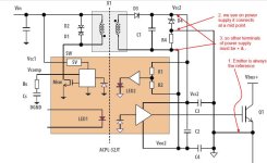
you haven't posted a schematic yet, so i will make some assumptions. i assume you are using lewbowski brain board and connecting it to gate driver board and your power mosfet is IRFB4110 (4 in parallel). now we have to identify all the delays.
1. starting at brain board, what is the delay difference between the PWM ON command and PWM OFF command (we start by assuming no deadtime). well the brain board is so fast probably the delay is less than 10ns, so we call this negligible.
delta_brain = 0s

2. between microcontroller on brain board and the gate driver logic input, what circuitry is there? i assume that you have only a resistor in between, specifically no low pass filter, no circuit chips doing something, nothing. so there is virtually no delay between the time it takes to turn one mosfet OFF vs. time it takes to turn ON. delta_PWM = 0s.

3. then PWM signal reaches input of gate drive IC, part number ACPL-32JT and we finally find our first elements of delay. for example, if the lower mosfet gate drive IC were asked to turn OFF, what is the worse case time it would take? on page 12 of datasheet we see delay to turn OFF worse case is 250ns and fastest to turn ON is 50ns. so delta_gateIC = 200ns. but look carefully, these values are given at 25decC and also there is a line just below talking about pulse width distortion (PWD) and deadtime distortion (DTD).
3a. effect of temperature. on datasheeet pg 12 it says on right hand side to look at figure 17. scroll down the sheets we see that propagation delay is affected by temperature, but not too much. that is, at any one temperature, the curves for delay ON and delay OFF change with about the same inflection which means although the ON time or the OFF time changes quite a bit (50%?) the DIFFERENCE between them does not change too much, at most looks like 50ns. so we can update our equation:
delta_gateIC = 200ns + temperature_affect = 250ns
3b. i think PWD means that the gate drive IC is not always accurate, that is when it receives a 1400ns PWM_ON command from brain board it may output anything between 1360ns and 1540ns. so we re-work the numbers by assuming worse case. if gate drive OFF command takes worse case 250ns then the distortion could add another 140ns to this. if gate drive ON command is as fast as 50ns then we could subtract 40ns from this due to distortion.. so the distortion delta is: 140ns - 10ns = 130ns, and we update our equations:
delta_gateIC = 200ns + temperature_affect + Pwdistortion_affect = 200ns + 50ns + 130ns = 380ns.
3c. i think deadtime distortion means that chip-to-chip there is variation. if lower gate drive receives 1400ns pulse width at same time as upper gate drive then it is possible that between the two there is possible a difference of -160ns to +60ns. note that this datsheet parameter is already given in differential units (delay high minus delay low). but what we are really calculating is delay low minus delay high, so we take the -160ns and consider it as +160ns and add this to our equation:
delta_gateIC = 200ns + temperature_affect + PWdistortion_affect + DTdistortion_affect = 200ns + 50ns + 130ns + 160ns
delta_gateIC = 540ns

interesting how the propegation delay of this gate drive just went from 250ns to 540ns eh?

4. next we consider the circuitry between gate drive IC and power switch. this depends a lot on your need of a boost stage or not. let's assume it does. what is the longest time it takes to propegate an OFF signal vs. shortest time to propegate an ON signal? i'm running out of time to answer this by reading datasheets and stuff, so i'm just going to assume the answer is 100ns (transistors tend to be fairly fast).
delta_boost = 100ns (not verified)

5. finally.. the power switch. how long does it take for mosfet to turn OFF vs. how fast to turn ON? so for turn OFF we see off delay of typical 78ns + fall time of 88ns for total of 166ns. similar for fast turn ON is 25ns + 67ns = 92ns. these numbers are at 25degC and also note these are typical time (datasheet does not specify worse case for some reason) so for sure we have to look at datasheet curves to see if we can find affect of temperature. except this datasheet does not have any! ugg.. we have to make a WAG (wild ass guess). so if the typical room temperature delta difference is 166ns - 92ns = 74ns, let's assume the variation on that is 50% so delta_IRFB4110 = 110ns. that is for ONE mosfet, but we assume 4 in parallel. what is the variation between MOSFETs? i don't know and it is not specified on datasheet, but it is a controlled element because you will make an effort to match the mosfets prior to installation for current sharing reasons. let's say the difference is small, around 20%. so
delta_IRFB4110 = 110ns + 110*0.2 = 130ns.

now we can add up our deadtime and multiply result by safety margine of 1.2 to get total deadtime:
deadtime = (delta_brain + delta_PWM + delta_gateIC + delta_boost + delta_IRFB4110)*1.2 = 770ns * 1.2 = 924ns.

which is JUST less than the desired 1us limit (see previous post).. rejoice! :D

now you can post the math for the leaf inverter result
 
Ok first.

Irfp4568 on delay 27 + raise time 119 = 146 off delay 47 + 84 = 131. Meaning it will turn off faster then on.
Irfp4668 on delay 41 + raise time 105 = 146 off delay 64 + 74 = 138 Meaning it will also turn off faster then on. I will come back once we are on the road to the ski hill.
 
Ixfk230n20t is delay on 41 + raise of 35 = 76 and delay off 104 + 29 raise = 133 for a delta of 57 ns.
Then the 1MBI800U4B-120 is 1200 ns + raise of 600 ns = 1800 and off 1000 ns + 300 = 1300 for a negative delta of 500ns. I can maybe set a low programmed dead time?
Question. I have not worked with igbts what is ton? tr? tr(i)? toof? tf?
 
don't forget to take temperature into consideration and also parallel mosfet timing (ALL mosfets have to be OFF before adjacent power switch turn ON).

i checked only Irfp4568 and see the timing is for "typical" conditions and also it says that even typical was taken at junction temp of 25C. so you have to make a guess at what the increased difference will be due to temperature. then also for parallel (leaf inverter does not need this factor).

for the leaf inverter module 1MBI800U4B-120, you did not do it correctly. remember we are after potential for PWM to be overlapped so we worry for longest time OFF vs. shortest time ON because that is the scenario that creates overlap.
Fastest time ON: 320ns + 100ns = 420ns
Longest time OFF: 1000ns + 300ns = 1300ns
for a delta of +880ns
** Now you have to read the datasheet to incorporate factor for temperature as well, for gate resistor value too.
Junction Temp effect on Timing:
there are two graphs that show timing due to junction temp. they are "Switching time vs. Collector current at Tj=25C" and right beside it "Switching time vs. collector current for Tj 125C'. so obviously the datasheet parameter values were chosen for the graph on the left, but what we should have used is the graph on the right. so make that change in the math. you'll have to use your technical ability to decifer if the worse case occurs at 0ams or at 800amps..

Gate Resistor effect on Timing:
notice the gate resistor graph, WOW, what a change! all of a sudden we see gate resistor as being major player for an IGBT (and probably mosfet).
so remember how Fastest time ON was 420ns? look at datasheet to see under what conditions that was given, we see junction temp of 25C (which we already know we have to investigate) and also gate resistor of 0.68Ohm. lol.. what's the chances that your gate driver design will have so low a resistor? that would create some crazy noise.. but honestly for big modules it is cutomerary to have between 1 and 5 Ohm, so not out of the realm of possibility. there are a couple of ways you could look at this.. by my feeling would be to pick a max gate resistor to make sure you can still hit 20kHz switching frequency and pray that the noise generated is not too bad.. you might recall from a PM i sent you a while ago saying that i think this module will have 3 Ohm max gate resistor.. now you know WHY i said that.
 
Yes you are right I'm trying to multi task. And after looking at the charts 3 ohms on the igbt would be a good place to start.
 
Quick question. DO I NEED to use the transformer they show or can we use something in place of it? Seems hard to get...
 
Back
Top