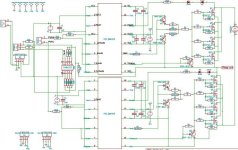
Arlo's power stage Leaf controller runs and drives page 103

zombiess said:
Arlo1 said:
zombiess said:
Arlo1, here is desaturation operation thanks to HIghHopes.
I don't agree with this. First off electrons flow from negative to positive. But also the pin for desat needs to reach 6.5v to activate desat so this voltage comes from the voltage drop measured of the mosfet. But the arrows don't show things in a way that make sense.

Follow the diagram, read up on it, it's not a voltage drop, it's voltage being generated just like it does through a shunt.
Voltage generated... as in a voltage drop measured across a known resistance which increases as amperage increases.
Zombies said:
Once he posted that diagram of the current flow it made a lot more sense to me on how it operated. The zener is needed for MOSFETs because the on resistance is a lot lower than an IGBT in most cases. The lower the RDSon of the power device, the higher voltage zener you need to make up the difference. The current through the power device generates a voltage and the desat circuit is measuring it like a shunt. More current + more resistance = more voltage, E=IR, this is what the desat circuit is looking at.

Forget the entire electron/hole flow stuff, it's not needed for this and even though that's the way electrons flow, you won't find many talking about it in that way.

I see you finally got your hands on that FLIR toy you wanted, hacked the firmware?

Can you test a TO-220. I read of one person doing a similar physical test to a TO-220 and 75A was the max and the legs started melting above that. I've also seen 75A referenced as a general rule of thumb in literature as the lead limit. Of course with short duration pulses with a long period in between you can go much higher. I've done > 200A through a single IRFB4115 in a bread board and 18ish gauge wire... for 100uS.
I will try to re-read your thread.... I will see if I have any TO220 fets to test with... I would bet 75 amps is not far off. Yes the FLIR is AWESOME :) Its hacked and the last hackable FLIR in Canada ! Gets yours fast because the new firmware is not hackable. Mine has options the E8 doesn't have! and yes with out the hack those pictures would have sucked major balls!
 
Arlo1 said:
Voltage generated... as in a voltage drop measured across a known resistance which increases as amperage increases.

LOL, yes, voltage drop. That's what I get for working on a gate driver with mind in magnetic flux mode and then typing a post, derp. Original posted edited.

I dont see myself needing a FLIR setup any time soon. Would be more of a toy to me, not that I wouldn't like one, I just can't justify the cost, even as a business cost. In a few years maybe, prices keep dropping.
 
Another question. So with isolated imputs do I want the run the high and low twisted together to the input of the driver or hi twisted with - and low twisted with -??
 
R3 - i was thinking that last night too. i believe you have it connected properly. should be value of ~47ohm it is not optional if you want Clamp circuit to work.. can you explain why?

i downloaded your desat schematic v1.1 but it just gives an error when trying to open in kicad.

what is the power dissipation in gate resistor calculated? and what Watt rating of your gate resistors did you chose?

you still need caps across your boost stage transistors.

R23 - R26 are not needed. it is sufficient to have ONE 4.75K resistor, connected between R21 & R8 to power mosfet source. put in parallel to this a "do not populate" pad of size 0805.. just incase you need a cap here to slow things down.

can you show high resolution picture of your input?

ps. i'm still waiting to see your math :)
 
the PWM signal is always twisted with it's reference on input side. since high side PWM and low side PWM have same reference (digital ground) actually its fine to put all cables in one twisted bundle if you wanted to. it is not all that critical even to be twisted on the input side of the gate driver (the brain board side), what i mean is a ribbon cable can work just as well as twisted pairs.

now if you were talking about flying lead connection on the power switch side of the gate driver, for example a connector to the gate/emitter of your leaf inverter module my comments would be totally different and more specific.
 
With 4 IXFK230N20T MOSFETS in parallel which have 378nc gate charge. At 50 kHz I get .0756 amps through the on transistor and .0756 amps through the off as well. I will post how I got the numbers later.
 
Arlo1 said:
With 4 IXFK230N20T MOSFETS in parallel which have 378nc gate charge. At 50 kHz I get .0756 amps through the on transistor and .0756 amps through the off as well. I will post how I got the numbers later.

4 of those in parallel have a 1512nC charge, Qg=378nC each at 10V, 15V will be higher, > 400nC, looks like it will be close to 500nC based on fig 10.

With a 2 ohm gate resistor, 15V on, 0V off and 30khz switching I'm getting 810nS switch time.
A peak gate current of 6.9A and an 880mA RMS
Power dissipated in the gate resistor is 1.55W so a min of 2W of resistor(s) should probably be used.
 
good catch on figure 10. arlo plans to use 12V power supply i believe, which you need to extrapolate figure 10 to discover Qg (worse case). but.. if there is votlage drop across boost stage & gate resistor.. then voltage applied to mosfet is about 10.5V ... which in the end is pretty close to what datasheet used for its Qg value. so maybe not too much need to extrapolate figure 10, perhaps 400nC.

zombiess.. for your math.. what gate resistor value did you assume? 15V/6.9A = ~ 2 Ohms ? your peak current is really high, i think there is a mistake

also.. are you taking into consideration that you may add an external G/S capacitor to slow switching down? 30nF you used...
 
HighHopes said:
good catch on figure 10. arlo plans to use 12V power supply i believe, which you need to extrapolate figure 10 to discover Qg (worse case). but.. if there is votlage drop across boost stage & gate resistor.. then voltage applied to mosfet is about 10.5V ... which in the end is pretty close to what datasheet used for its Qg value. so maybe not too much need to extrapolate figure 10, perhaps 400nC.

zombiess.. for your math.. what gate resistor value did you assume? 15V/6.9A = ~ 2 Ohms ? your peak current is really high, i think there is a mistake

also.. are you taking into consideration that you may add an external G/S capacitor to slow switching down? 30nF you used...

Yup, you caught my typo, the math was done with a 2 ohm gate resistor. Looking at the switching di/dt involved here I really start to worry about keeping gate ringing under control. Slowing it down with a G-S cap seems like the only way to control it because the gate resistor value is so small. I only bring this up because of my experience working small scale with it.

I did not take a G-S cap into consideration, so there is some more peak amps needed.

BTW, what method is better to control the on/off time of the gate. Working under the assumption the gate driver had the current deliver capability, is it better to have a lower gate resistor and higher G-S cap to achieve desired D-S switching time or is it better to have higher gate resistor, lower G-S cap? I was thinking lower resistor, high G-S cap because I noticed it really killed off any overshoot, but I'm also thinking the gate voltage could possibly rise faster with a lower gate resistor and then the G-S cap would extend the miller plateau. I have not had a chance to experiment with this idea yet, but I figured you've probably poked around with this idea in the past. Your thoughts?
 
How do you calculate the peak current?
 
Highhopes here is a more updated and cleaned up version. IM going to try downloading a PDF creator as well.
 

Attachments

  • Mosfet desat (800 x 506).jpg
    Mosfet desat (800 x 506).jpg
    70.6 KB · Views: 3,931
Sweet I figured out how to do it strait from Kicad.
I added R42 and R43 for a place to put a ferrite bead if I need.
 

Attachments

  • desat v1.1 .pdf
    67.8 KB · Views: 125
HighHopes said:
R3 - i was thinking that last night too. i believe you have it connected properly. should be value of ~47ohm it is not optional if you want Clamp circuit to work.. can you explain why?
Yes the clamp feature needs to use Vout to measure the gate voltage to make sure the gate is below the miller plateau to clamp the fet to VEE
 
Arlo1 said:
How do you calculate the peak current?

I made a gate driver spread sheet to make life easy for me, but here are the formulas.

effective gate capacitance
Ceff = Qg/delta_Vdr

Time to charge mosfet gate
tpON = 1.4*Rg_ON*Ceff

Time to discharge mosfet gate
tpOFF = 1.4*Rg_OFF*Ceff

peak current into the gate
IpON = (VON-Vg)/RgON

peak current discharged from the gate
IpOFF = (VOFF-Vg)/RgOFF

RMS current into the gate
Irms_ON = i_peak * Square_root(tp*freq/3)

RMS Current off from gate
Irms_OFF = i_peak * Square_root(tp*freq/3)

Total RMSs current in/out of the gate if only a single resistor is used
Irms_OFF = i_peak * Square_root(tp*freq/3)

Power dissipated in on gate resistor
PRgON = Irms_ON^2*RgON

Power dissipated in off gate resistor
PRgOFF = Irms_OFF^2*RgOFF

power dissipated in a single resistor setup
PRgTOTAL = Irms_TOTAL^2*RgON


To size the gate power supply
Idrive = Qg * fsw - Average Current supplied to the gate driver

Pg = Idrive * delta_Vdr - mW required by the gate driver setup

Now go forth and multiply... and divide... and all the other fun math functions :mrgreen:
 
Thanks Jeremy that needs to be a sticky for all the forum.

Now I just realized one thing to be careful of when the Driver senses desaturation it will try to slowly pull the gate down before using the clamp. But If I use a boost stage I will want to be careful not to use to low of a resistor on the off transistor correct? Because with the boost stage it will not really allow the driver to control the speed of the on and off switch.
 
Sorry arlo1 but I don't understand what you are asking above, at least not in my experience with the td350e driver. With desat I never had to worry about the gate during a fault, the driver takes care of everything which is why I like it.

Your off time is controllers by your gate resistor(s). You can use separate on/off resistors with a boost stage just like normal. The miller clamp still engages even during a fault. Usually around 2v.
 
In the appnote it mentions how it softly shuts off the igbt or mosfet during desat before applying the clamp to prevent big spikes. And it mentions its done internally. I will try to find what page later.
 
Arlo1 said:
In the appnote it mentions how it softly shuts off the igbt or mosfet during desat before applying the clamp to prevent big spikes. And it mentions its done internally. I will try to find what page later.

That is only for 2 level turn off and that feature can not be used with a high PWM frequency. I'm not sure what the max is without doing some math. If you want to switch at 30-40khz I believe you will have to disable the 2 level turn off, but I could be wrong, it might still be usable at 30khz if you make the timing period short. The downside is the shorter the timing period the larger the Vce / Vgd spike ends up being, but anything is better than nothing.

Mr. Hopes will hopefully chime in with some of his experience using the 2 level turn off and the max PWM freq it's good for.

Luckily you get to pick and choose which features you want to use.
 
Top right side of ACPL_333J DATA sheet page 20.
Title "slow igbt gate discharge during fault condition."
"When a desaturation fault is detected, a weak pull down device in the ACPL_333J output drive stage will turn on to "softly" turn off the igbt. This device slowly discharges the igbt gate to prevent fast changes in the drain current that could cause damaging voltage spikes due to lead and wire inductance."
 
is it better to have a lower gate resistor and higher G-S cap
- it is best not to need the G/S cap at all and control switching speeds only by gate resistor. that's how i did it always. adding G/S cap is new to me, but seemed to work for only penalty of needing slightly bigger power supply. i remain hopeful that G/S cap does not intruduce an avenue for noise to couple into the gate drive IC .... :!:

zombies, your math does not take into consideration parallel mosfets. Ceff also should include gate drive cap G/S.
for gate power supply, need parallel mosfet & gate cap G/S added into the math (i already did it and calculated result for arlo's design).

I did not take a G-S cap into consideration, so there is some more peak amps needed.
adding G/S cap does not increase peak current as the max theoretical is already defined by Ohms law, V/Ohm = Ipk --> 12V/2 Ohm = 7Amps. technically speaking.. ;P
adding this cap will however increase the average drive current which affects how big the power supply watt rating needs to be. as more average current flows into gate resistor then also you will need incraesed watt rating.
i feel like i am picking on you tonight..
 
arlo, your PDF is 1000x times easier to read!

VE & VEE of gate drive IC.. are they supposed to be tied together for unipolar power supply?

R39 is taking a signal from the Mosfet side of gate drive IC over to the digital brain side of gate drive IC. this is a STRICT NO NO! you must always maintain isolation. my guess is that you probably do not realize you have two ground references that are totally separated (as they are supposed to be). does this make sense?
 
"soft" shut down, you are both correct. in TD350 the soft shut down occurs at EVERY switch no matter if there is a fault or not. on the plus this means it is more tolerant to DIY construction, but on the negative it impacts what your normal switching frequency can be. ACPL-333J has also a soft shut down but it is engaged only when a fault is detected so it does not impact normal operation (does not limit your choice of switching frequency).

maybe this makes it sound like ACPL-333J is better.. perhaps it is, but keep in mind that TD350 is like 10 years old and has recently been moved into "mature" status. TD350 is a proven device which passed the test of time. we don't know yet how ACPL-333J will be, our faith is in the company and their few years of practice in this field.

application note AN 5315 goes into detail how it works and more importantly how it works with a boost stage.
"To increase the IGBT gate drive current, a non-inverting current buffer, Figure 5, can be used. Inverting types are not compatible with the desaturation fault protection circuitry and should be avoided."
hmm... looks like something you need to check. do you have a non-inverting current buffer?
 
AN 5315 had another interesting note about boost stage transistor selection:
"The MJD44H11/MJD45H11 transistor pair is appropriate for currents up to 8 A maximum. The D44VH10/D45VH10 transistor pair is appropriate for currents up to 15 A maximum."

keep those part numbers in your lab book for future reference
 
here are some comments for you to consider.

note, i have not reviewed the digital brain side of your schematic, i was just looking at power mosfet side. ran out of time and now i need my beauty sleep :)
 

Attachments

  • desat v1.1 Comments.zip
    1.3 MB · Views: 180
HighHopes said:
arlo, your PDF is 1000x times easier to read!

VE & VEE of gate drive IC.. are they supposed to be tied together for unipolar power supply?

R39 is taking a signal from the Mosfet side of gate drive IC over to the digital brain side of gate drive IC. this is a STRICT NO NO! you must always maintain isolation. my guess is that you probably do not realize you have two ground references that are totally separated (as they are supposed to be). does this make sense?
R39 is 100% mandatory this is how the controller reads the 3 phase positions see lebowski's thread.

Are you talking about the low side VEEL? and the Hi side VEE yes they need to be separated and I know why.. For others reading this is it because VEE is connected to the phase wire which is a floating voltage and if the two VEEL and VEE were connected shit will blow up! :)
But as for "your guess" I really appreciate your help but I'm not an idiot.
VE and VEE can be connected when not using a negative voltage to shut the fets off. IN the leaf inverter they are separate.
 
Back
Top