Building the Best Controller

rhitee05 said:
IRFP4368 is a good choice in TO-247 for 75V.

Duly noted:
IRFP4368PbF: 75V, 195A!

So what do you think people? Toss out the 12-FET and just go with a 6-Fetter? There is P L E N T Y of juice here and if we support Off-The-Board FETs I'd say the concept is baked.

~KF
I just have to price out one of those 150V buggers though...
 
As (many) have already noted, the headline current ratings on the datasheets bear very little resemblance to reality. You really need to do a heat calculation under PWM conditions to get a proper estimate of current handling. Even an I^2*R calculation for continuous current is optimistic since there are additional switching losses.
 
ZapPat said:
That's an interesting document (AN-1140)- it probably describes best our true current handling bottleneck. Thanks for posting the link, Eric.

I read this app note as saying that our real problem is not so much the lead size itself, be it TO-220 or TO-247, so much as the nature and quality of the contact area's between the FET and the PCB. Here's an additionnal quote from the app note that sums up the conclusion they reached:

IR doc AN-1140 said:
The primary constraint upon the amount of current is the temperature of the source contact on a printed circuit board.

There's also another problematic too, which is the PCB's current handling capacity. Expecting much over 140A out of even a 3oz PCB will be pushing it I think. Bus bars would solve this issue, and if some sort of mechanical source pin clamping setup (instead of soldering) could be made then the source connection point main current bottleneck described above could be eliminated too.
I can confirm that the point at which the FET connects to the PCB is critical. I easily handle over 200A on my 3oz.-Cu PCBs in my electronic loads (i.e., continuous heating) but that's only after spending a lot of time making sure that the thermal resistance from the FETs to the PCB is as low as possible. TO-220 FETs are useless for this as the lead-spacing is too small. TO-247 and TO-264 work great.

Proper use of multiple layers of copper, thermal vias between layers, sizing the holes VERY carefully for the FET leads (you cannot depend on solder for heat transfer!!!), and maximizing the amount of copper available within 0.2" or so of each FET lead (and across the entire board) are critical, but are done without too much trouble. While proper cooling via a heat sink is critical, you can ensure that the max. current rating for those FET leads can be reached with good PCB layout.

Personally, I wouldn't even consider anything less than a 4-layer board for this. The other two layers can significantly ease any layout compromises, greatly reduce the inductance of the traces, and will do amazing things for spreading out the heat. This is a high-end controller, no sense trying to save a little bit of $$$ on the PCB when 4-layers provides so many benefits.

And, while easy to dismiss initially, I wouldn't immediately discount the use of a metal-substrate PCB, typically aluminum under very, very thin polymide layers holding the copper for the traces. This allows you to use surface mount components (the FETs), which are easily reflow- or hand-soldered, and gives you a very large, insulated metal surface to mount to a heat sink. This can significantly ease assembly, reduce the parts count (no mounting hardware), and further reduce system inductance. It also allows the use of smaller, less expensive FETs which are spread out on the PCB to achieve low thermal resistance numbers. Yea, you'll have a lot of them, but that's the idea. Common, inexpensive FETs can be used and lots of them helps to spread out the heat. This makes the metal substrate very efficient at transferring the heat to the heat sink.

You'll have to run the standard cost (including heat sink, mounting hardware, etc.), FET size, driver requirements, thermal resistance, etc., numbers but it can make this thing MUCH easier to build. And since the PCB has to be 3rd-party manufactured, it can be worth considering. :)
 
Thanks for your input John. We normally seem to agree 100% on most everything.
I do agree if you wanted to go SMT, the aluminum clad board would the only way to go, but I don't think its a wise choice for this application.

The busses can be made so simple. I've got a big stack of heavy copper sheets and a CNC machine that cuts out busses and traces like candy. If you guys want a run of 100 or something for a bus layout that is made to make a super compact 6fet with those dreamy little IXYS fets and give a bunch of cap locating holes in the power rail busses or whatever, it would be my pleasure.
 
* MMIX1T550N055T2: 55V, 550A
* MMIX1F520N075T2, 75V, 500A

I see now that IXYS finally put out a media release acknowledging these FET's existence on the 7th October, but I'm yet to see a supplier who stocks them for sale in small quantities. Is it still early days? Are you confident these will soon be available to non OEM's in small quantities? I agree these are the FET of choice if they become freely available. ~$11 a pop is a bargain if we can get them around that price, however I'm skeptical that Digirip and Newfark wont mark them up threefold.

BTW. It's interesting what turns up in the recommended application list for these FET's;

"Suitable applications include: DC-DC converters, UPS, electrical bikes, motor control, solid state relays, and high-current industrial battery charging applications." http://forums.digitalmedianet.com/articles/viewarticle.jsp?id=1221055

Luke, are you sure you didn't let slip your application intentions when you were talking to your IXYS rep about ordering a bunch for "Microsoft business use" :lol:
 
John, love the idea of using distributed SMT for a controller. After solving the drive problems you could build a multi KW controller that fit in your shirt pocket! To use it as the primary driver for this project would probably require a total rethinking of the design though, wouldn't it. Not that that would necessarily be reason to reject the idea.

lfp, you're basically suggesting cutting out the traces for the ultimate single sided PC board, right? 1oz, 3oz, how 'bout 30oz?! A grown up version of the xacto knife 'pc' board that was the first effort of many of us. :)

Both ideas could/would be alternatives to the big industrial chassis mount blocks wouldn't they. As far as the controller is concerned, the main consideration would be making sure we could drive them. I expect the CNCed bus bars would be the easiest to prototype.

How about laying the transistors flat and soldering the leads to the copper like SMT. Lots of solder area for both electrical and heat conduction. Changes the heat sink arrangement, not that that's been discussed. Could we sandwich/clamp the part between heatsinks? How much thermal conductivity is there to the face of the part.

Much progressive and INTERESTING discussion. I like it.

Bob
 
oldswamm said:
John, love the idea of using distributed SMT for a controller. After solving the drive problems you could build a multi KW controller that fit in your shirt pocket! To use it as the primary driver for this project would probably require a total rethinking of the design though, wouldn't it. Not that that would necessarily be reason to reject the idea.

lfp, you're basically suggesting cutting out the traces for the ultimate single sided PC board, right? 1oz, 3oz, how 'bout 30oz?! A grown up version of the xacto knife 'pc' board that was the first effort of many of us. :)

Both ideas could/would be alternatives to the big industrial chassis mount blocks wouldn't they. As far as the controller is concerned, the main consideration would be making sure we could drive them. I expect the CNCed bus bars would be the easiest to prototype.

How about laying the transistors flat and soldering the leads to the copper like SMT. Lots of solder area for both electrical and heat conduction. Changes the heat sink arrangement, not that that's been discussed. Could we sandwich/clamp the part between heatsinks? How much thermal conductivity is there to the face of the part.

Much progressive and INTERESTING discussion. I like it.

Bob

The real challenge is the heat build up between the junction and the bit of metal on the package. The poor internal thermal conductivity of the old-style three lead packages is what tends to create the problem, primarily, I think, from uneven heating between FETs which then leads to unequal current sharing and failure. The newer packages are much better at getting heat from the junction to the case/heatsink attachment point, so much so that they may well reduce the need for big heatsinks to the point where they may not really be needed. I've often thought that using machined copper bus bars as heatsinks would be an elegant way to go, combining the function of two parts.

A typical TO220 package has a thermal resistance of maybe 0.5 deg C per watt between the junction and the case, TO247 devices are a little bit better, but both have a relatively high case to heatsink thermal resistance, due to the limited area in contact with the heatsink and the way that the die is mounted inside the package. By contrast, the FETs LFP linked to are around 0.18 deg C per watt junction to case, the big ones he and I have are 0.08 deg C per watt junction to case.

Jeremy
 
Jeremy Harris said:
The real challenge is the heat build up between the junction and the bit of metal on the package. The poor internal thermal conductivity of the old-style three lead packages is what tends to create the problem, primarily, I think, from uneven heating between FETs which then leads to unequal current sharing and failure. The newer packages are much better at getting heat from the junction to the case/heatsink attachment point, so much so that they may well reduce the need for big heatsinks to the point where they may not really be needed. I've often thought that using machined copper bus bars as heatsinks would be an elegant way to go, combining the function of two parts.

A typical TO220 package has a thermal resistance of maybe 0.5 deg C per watt between the junction and the case, TO247 devices are a little bit better, but both have a relatively high case to heatsink thermal resistance, due to the limited area in contact with the heatsink and the way that the die is mounted inside the package. By contrast, the FETs LFP linked to are around 0.18 deg C per watt junction to case, the big ones he and I have are 0.08 deg C per watt junction to case.

Jeremy

Nothing we can do about internal heat except cool the package as much as we can, or abandon the 3 lead parts entirely.
I'm thinking that this controller project should be geared toward that eventual abandonment (we're trying to think of the future, right).
Design the output board as a driver for the external chassis mount parts, but try and make it so those of us with modest needs could solder fets directly to the board. Perhaps final driver transistors could be interchanged with fets, in alternate versions of the board. Just solder in the parts you need, and leave other spaces empty.

How are you guys driving those big block fets now?

Bob
 
I think that you can build it on plain two layer, 3 oz copper boards. My welder (and other designs) uses fat drain and source busses on each side of the board, connected by vias. The MOSFET gates are not wired to etches on the boards. They are hand wired by flying leads. This lets you dedicate uninterrupted PCB buses to the high current path on a two layer board. Picture at http://endless-sphere.com/forums/viewtopic.php?f=2&t=2633&start=570#p280216 Also, I do not trim the MOSFET leads. The extra metal helps a little with the heat.

On the welder, I use 18 x IRFP2907 FETs. It produces 20,000 amp pulses (granted at a very low rep rate) and the FETs are not heat sinked. They have zero temperature rise, even after firing 1000 welds in under 30 minutes.
 
Jeremy Harris said:
The real challenge is the heat build up between the junction and the bit of metal on the package. The poor internal thermal conductivity of the old-style three lead packages is what tends to create the problem, primarily, I think, from uneven heating between FETs which then leads to unequal current sharing and failure. The newer packages are much better at getting heat from the junction to the case/heatsink attachment point, so much so that they may well reduce the need for big heatsinks to the point where they may not really be needed. I've often thought that using machined copper bus bars as heatsinks would be an elegant way to go, combining the function of two parts.

A typical TO220 package has a thermal resistance of maybe 0.5 deg C per watt between the junction and the case, TO247 devices are a little bit better, but both have a relatively high case to heatsink thermal resistance, due to the limited area in contact with the heatsink and the way that the die is mounted inside the package. By contrast, the FETs LFP linked to are around 0.18 deg C per watt junction to case, the big ones he and I have are 0.08 deg C per watt junction to case.

I can't disagree with this too strongly, because you are correct that this is a limiting factor for these packages. But, a show-stopping problem for a 10 kW controller might be only a minor nuisance for a 1 kW controller. A TO-220 or TO-247 FET might have a total junction-to-sink Rth on the order of 1 C/W. But that's not really a huge deal if each FET is dissipating 10-15W, that's only a delta T of 10-15 deg C. Not a big deal, not a huge impediment to cooling. The heatsink will still be the limiting factor. In a heavy-duty controller where you want to dissipate 50W or more per FET, that's a different ball game.

I applaud what you guys are trying to do with those big FET packages, they are 100% the way to go for high-power. But there's nothing wrong with the TO packages for "normal"-powered controllers with a little attention to thermal management. There's no need to use a $15 part when a $3 part will do just fine.

I would actually love to build a small controller using D2PAK-7 packages one of these days. It may be a "wimpy SMD package" but you could make a great mid-power RC controller using 60V parts with very low Rds values good for a few kW. The packages have several short leads in parallel, so the package parasitics are small and you could switch them very quickly. I think it would work quite well, especially if put on a metal-substrate PCB.
 
The last time I priced metal substrate boards, they were an order of magnitude more expensive than heavy copper fiberglass boards... YPMV...
 
texaspyro said:
The last time I priced metal substrate boards, they were an order of magnitude more expensive than heavy copper fiberglass boards... YPMV...
They are a lot more expensive but using them eliminates a lot of other expenses (FET mounting hardware, FET insulators) and you get wonderfully distributed heat sources. Depending on the setup, you can save a great deal of money using a metal-substrate PCB.

Not saying it's the best choice, just that it can be a better one for some setups. Worth doing the math IMHO for any project being considered though. :)
 
oldswamm said:
How about laying the transistors flat and soldering the leads to the copper like SMT. Lots of solder area for both electrical and heat conduction. Changes the heat sink arrangement, not that that's been discussed. Could we sandwich/clamp the part between heatsinks? How much thermal conductivity is there to the face of the part.

Much progressive and INTERESTING discussion. I like it.

Bob
Soldering the leads directly to copper bars can be done successfully, but you're probably going to exceed the temperature specs for the FETs and somebody, if not a few people, are going to damage their FETs. IMHO, not really needed since only a little bit of heat comes out the leads vs. the "rear" metal mounting plate. Better to spend the time and $$ on making the thermal connection between the mounting plate and the heat sink as efficient as possible and then sizing the heat sink properly to keep the junction temps below 80% of the rated max (for good reliability).

Regarding sinking the epoxy face of a FET...
Unfortunately, almost no heat can be taken out from this side as the thermal resistance to the junction is very, very high. :cry: :cry:
 
CamLight said:
Not saying it's the best choice, just that it can be a better one for some setups. Worth doing the math IMHO for any project being considered though. :)

My gut says it's way overkill for the app. 3 oz copper was under 20 cents/sq in. Metal was over $5. Could have just been the supplier, but I suspect not. At 5 bucks a sq in, you can buy a lot of fet hardware, etc.
 
CamLight said:
Soldering the leads directly to copper bars can be done successfully, but you're probably going to exceed the temperature specs for the FETs and somebody, if not a few people, are going to damage their FETs. IMHO, not really needed since only a little bit of heat comes out the leads vs. the "rear" metal mounting plate. Better to spend the time and $$ on making the thermal connection between the mounting plate and the heat sink as efficient as possible and then sizing the heat sink properly to keep the junction temps below 80% of the rated max (for good reliability).
Yea, I wasn't thinking of the amount of heat to bring a large mass of copper up to temp, for soldering. :)
CamLight said:
Regarding sinking the epoxy face of a FET...
Unfortunately, almost no heat can be taken out from this side as the thermal resistance to the junction is very, very high. :cry: :cry:
What I assumed. The best heat conductive epoxy is still and insulator.

Has anyone found any fets in sot-227? 3 of those with dual fets in them, for an e-bike........ :D

Bob
 
I made a little video showing how to mount large banks of large FETs to heavy copper bus bars.

Requires all sorts of tricky tools and skills to use.
Or, maybe just 3 very simple tools. ;)

Normal stove-top electric burner on your oven.
$4 jar of solder paste (yes, $4 shipped!)
Little flat steel plate, about 1/4" thick or so, and at least bigger than the FET layout by enough to leave handholds on each side. A little 6x10" 1/4" steel plate that costs about $2 would be fine (or aluminum scrap plate, or pretty much

Arrange the FETs however you like them, in the case of these slick IXYS fets, just screw them down to the heatsinks in the right positions etc, because the connection side is on the non-sinked side of the package (which is what makes them dominate all other SMT parts).

Set the little chunk of steel on the oven burner, and make sure it over-hangs enough to get a hand with a hot-pad on each side to lift it. Lay out your bus bars on the steel plate surface. A little tracing paper with the diagram layed out on the top of it and a bright light seems to work well if you've got a super elaborate layout to get all perfect, normally it's not too tough to just eyeball it, or have a few marks on the steel plate for alignment. If you're super fussy, you can kapton-tape down areas you're paranoid about sliding around magiclly or whatever.


Once it's all layed out, put a tiny-tiny little dab of solder paste on some of the pieces in some areas. These are just temp indicators to let you know the temp is right. If you have a little IR temp gun, that works fine too, but the little temp indicator bits of paste work very well, not critical to have the IR temp gun.

Set out a folded soaking wet towel on the counter next to the stove.

Apply the solder paste to the FET legs you wish to be connecting. For the IXYS fets, this means just bend the gate leg out of the way, and/or all ready have your 6 wires on them and bent up out of the way if your buss bar setup is going to be blocking access to them.

Turn on the burner, watch the indicator dabs of solder paste, when they've all melted, switch off the burner, watch your alignment marks, and set the FET/sink array down onto the bus bars. The solder paste melts and wets almost instantly on contact. Have those hotpads ready, and lift up the steel plate and set it down on the very wet towel. Steam, steam, yadda yadda, now you just perfectly soldered up all your FET connections to heavy copper buses while putting even less heating into them than a normal solder bath could ever do, and WAY less heat into them than any lead-free process would do.

Also, it takes about 5mins for the whole soldering process. If you were going to do batches of them and had 2-burners and steel plates setup, you could likely assemble all the high current FET stage connections in maybe ~2mins each.

Soldering Bus bars with a solder iron can be AWFUL!
Soldering Bus bars with a stove burner = bliss, speed, and simplicity.


I've got loads of copper sheet here, it's maybe 1/16" thick, and my CNC can cut it into a snowflake pattern with ease. Room on my CNC's table to put down the double sided tape and do a run of maybe 40 sets of bus bars at a time.

I will gladly make them for you guys at no cost, not even materials cost (I got the copper in an auction lot for dirt cheap anways). BUT! I freaking HATE mailing things, so if I'm going to do it, all the pieces get shipped in a big flat-rate box to somebody that likes writing down addresses and going to the post office etc, because it seems to be something I really struggle with doing for some reason.
 
texaspyro said:
My gut says it's way overkill for the app. 3 oz copper was under 20 cents/sq in. Metal was over $5. Could have just been the supplier, but I suspect not. At 5 bucks a sq in, you can buy a lot of fet hardware, etc.
Agreed! That pricing seems high to me though but I have forgotten what we were quoted for a 15 sq. in. board we were considering last year. Definitely not $75 though (500pc. lots).

We do have to figure in assembly time along with the great thermal numbers (which can be absolutely critical for reduced sizing and pushing a device to the limit in the smallest package size). Especially if a run of machine-assembled FET boards are done....very low cost compared to time spent hand assembling, mounting, etc. But, then it's not nearly as DIY. :)

I agree that it's probably not worth it for this app as we have lots of room and lots of different approaches folks want to take towards parts spec'ing and the build. A more-generic thru-hole board (for the FETs at least) will do great here.
 
Any thoughts on the above described bus assembly method John?
As a guy with lots of real world experience in dealing with FETs, I greatly value your input. :)
 
Some thing else to consider (yea, yea, still on the SMD-approach :), will drop it after this )...

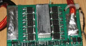
Even a standard 4-layer board can handle a huge amount of heat with surface-mounted FETs if there's a bit of room for some metal. The image below shows the prototype for a BMS I did using 9mOhm P-FETs for the primary safety switch (about 40-cents each). The FETs reached a junction temp of about 100C in 9 seconds at 150A without that block of aluminum (1/2" x 1/2" x 1-1/4") but they can go for a couple of minutes before reaching 100C with the Al block sinking the heat away from that plane of copper between the back-to-back FETs (about 3/4" wide). And that's even with a solder mask between the aluminum and the top copper (2 oz. top/btm, 1oz. internal).

IMHO, using a dense array of thermal vias to bring the heat to the layers below, and a heat sink against the bottom copper, would only increase the junction temp a few degrees vs. cooling from the top (this is what we'll be doing for the 2nd Gen board). You get to remove heat from the entire bottom plane of the PCB too so the FETs can be spread/staggered to take advantage of that (where possible). And no expensive metal-substrate PCB needed.

Just tossing out an idea. :)

BMS-SB-01-#001-in-testing.jpg
 
liveforphysics said:
Any thoughts on the above described bus assembly method John?
As a guy with lots of real world experience in dealing with FETs, I greatly value your input. :)
I LOVE IT!!
I was originally worried that the thermal shock on the FETs was pretty high. But, then i realized it's probably no worse than hand soldering?

But it might perhaps be subject to more variability than hand soldering to a PCB? I think the method will work great for those who take their time and have the skill to do it right, it could be problematic for others. Unless a bunch are manufactured by someone with the skill to do a great job (ahem, you). :D

The only thing that I see being a (remote) problem is that I really like to see mechanical connections in addition to thermal and electrical ones. That's just me though...reliability, reliability, reliability. If the FETs got too hot and desoldered themselves in a controller while riding, the results could be epic. :shock: More epic than any other controller that pops a FET? I don't know.

Hmm....actually, if the FETs got that hot, the rider should have their controller blow up anyway for thinking they could undersize it so badly!! :twisted: :twisted: A thermal switch on the bus bar could completely solve this problem I guess.

In the end, I guess I would like to see some type of clamp across the FETs, screwed between each FET. But, that feature could built into the controller by clamping the front face of the row of FETs to the inside face of the controller case (with screws from outside the case into the bus bar) or to the rear of another FET bus bar.
 
We could have a FET stage assembly party at my place I guess. It's not like I've got a wife to complain about it. lol

I would rather not get stuck doing a few hundred of them alone though. lol

But if Kingfish and some other local folks wanna come by make a day of doing the FET stage assembly with me, I'm down for that. We could make it a BBQ or something as well. :)

I'm serious about not being the guy that has to mail these things out though.
 
CamLight said:
Hmm....actually, if the FETs got that hot, the rider should have their controller blow up anyway for thinking they could undersize it so badly!! :twisted: :twisted: A thermal switch on the bus bar could completely solve this problem I guess.
I was thinking of how hard it would be to change one when it blew, then realized what a challenge it would be to blow one. :lol:

I can't say I like filling and labeling boxes, but if it came to that, I have to admit THAT'S something that falls within my abilities, and would probably be willing to volunteer. :)

Bob
 
liveforphysics said:
We could have a FET stage assembly party at my place I guess. It's not like I've got a wife to complain about it. lol

I would rather not get stuck doing a few hundred of them alone though. lol

But if Kingfish and some other local folks wanna come by make a day of doing the FET stage assembly with me, I'm down for that. We could make it a BBQ or something as well. :)

I'm serious about not being the guy that has to mail these things out though.

BBQ?!? That's my middle name :lol:

Love to help. If we're still considering SMDs, the only item that has me hesitant to committal is that we haven’t sourced units matching the spec range ≤ 150V.

I do appreciate the alternatives to metal substrate.
~KF
 
Kingfish said:
liveforphysics said:
We could have a FET stage assembly party at my place I guess. It's not like I've got a wife to complain about it. lol

I would rather not get stuck doing a few hundred of them alone though. lol

But if Kingfish and some other local folks wanna come by make a day of doing the FET stage assembly with me, I'm down for that. We could make it a BBQ or something as well. :)

I'm serious about not being the guy that has to mail these things out though.

BBQ?!? That's my middle name :lol:

Love to help. If we're still considering SMDs, the only item that has me hesitant to committal is that we haven’t sourced units matching the spec range ≤ 150V.

I do appreciate the alternatives to metal substrate.
~KF


These guys would make a mean mean <150v 6-fet controller (I've mentioned them before in this thread). Outstanding Pd and Rth, and a great RdsOn (not that it matter much compared to the Rth and Pd) for a 150v fet.

http://www.mouser.com/ProductDetail/Ixys/IXFX360N15T2/?qs=sGAEpiMZZMuRdXZgphLdVmRgq2vYKSVI

But, they are not isolated packages, and they are 3-pin style, so the layout isn't nearly as simple as those little IXYS 1"x1" pucks that don't have need for a PCB. These would need a PCB, and mechanical screw mounting etc.

Still, there are no 150v FETs in a decent price range and size that match them. They would be more DIY friendly to people who use soldering irons to solder, then insulate with a layer of kapton, and screw to a sink. OR, this would be a good FET to use mounted by it's drain tab soldered directly to an aluminum PCB as John was talking about. I think I would want to go with a 12-fet design if this path was taken though, shares the trace burden and spreads the thermal burden better, because these aren't quite miracle FETs like the 55 and 75V little pucks. :)

$14.26 in quantities of 100 from Mouser, which knowing mouser, means I can likely source them for $10-12 each.
 
Back
Top