DIY Programmable BMS (now using ATtiny/Arduino)

I wasn't aware that the ATmega32u4 had a different ADC than the ATtinys, I'll have to read up on it some more. I decided on the ATtiny25/45/85 due to the fact that it will operate down to 1.8V supply (so it can be powered directly from the cell) and is available in both surface mount and through hole. Depending on how big the pcb ends up, I may switch to the ATtiny44/84 since it's a bit cheaper, albeit larger.

I've got a few parts on order to breadboard a proof of concept and measure the overall power consumption. In theory it should be pretty low as the cpu can be put to sleep between measurements. Low enough at least that it will be negligible. I'm guessing 10-15 microamps should be achievable, which might as well be zero since it's so far below the self discharge rate.

I've got a proof of concept cell voltage measuring program up and running on an Arduino Uno (ATmega328), using the internal 1.1V reference. Accuracy is pretty bad though, since the 1.1V internal reference is around +/- 10%, but at least I can use it to verify my code works. I ordered a few 1% 1.2V references from TI, combined with the inherent gain/offset errors in the avr's ADC, I should be able to achieve better than 0.02V accuracy. I'll post more on the theory side of things later, but for now it appears that the actual circuit will be pretty simple.
 
Quick update on using an ATtiny85 for a BMS... I'm tackling the more difficult problems first, then moving on to the simpler ones. In this case the difficult problems are monitoring the cell voltage with only the use of a precision reference (ie no resistive voltage divider) and making the microcontroller go to sleep when not doing anything. Balancing is simple, just switching a pin between high and low to turn a transistor on and off.

To deal with the problem of measuring cell voltage, I initially hoped to use the internal 1.1V reference of the avr. I knew it was not very accurate, but I had heard that they were at least stable and could be calibrated fairly accurately. Since I don't need much more than about 20mV accuracy, I had hoped this would work. Unfortunately the measurements were very unstable, and I was measuring the supposedly 1.1V reference at about 1.35V, way outside the +/-0.1V it was supposed to be.

Since my 1.2V reference chips haven't arrived yet, I built up a 2.5V precision reference from a TL431 I had laying around to test the concept. Compared to the internal reference it was night and day. I was able to measure the supply voltage down to about +/-0.01V and unlike the internal reference that wandered quite a bit, the external reference stayed stable.

I did a bit of work getting the microcontroller to sleep between measurements, which should bring the average current draw down around 10 microamps (or possibly even lower). Overall I'm feeling pretty good about going this route instead of the pure analog method. I will probably switch to the ATtiny84 (or ATtiny44) due to the large number of I/O pins. Doing that should allow me to add an ICSP header, allowing on-board reprogramming of the chip.

Lastly, feature set... I want the microcontroller version to basically replace the analog version, with the only real difference being (hopefully) much simpler assembly and configuration. That said, this is what I'm planning.

1. Similar to the analog design, be open source so users can manipulate it at will.

2. Compatible with any cell chemistry operating within 1.8V and 5.0V. LiFePO4, Lipo, LiMn, LiCo, etc. Could also be used with supercaps.

3. LVC user configurable anywhere from 2.0V and up. When below LVC, the micro triggers an isolated output that can either pull the controller shutoff signal low directly, or be detected by another microcontroller (Arduino or whatever you prefer). To lower power consumption, this could be pulsed, or just held constant.

4. HVC and balancing configurable similar to LVC. When HVC is triggered, the optoisolator could also be turned on to let the charger know that HVC has been reached and to throttle the current back. Also possible is variable duty cycle for the balance resistor depending on voltage level, ie "soft balancing of 10% or so at 3.5V and then full blast 100% at 3.65.

Really, the possibilities are endless. I'd love to hear more feature suggestions, although keep in mind that the basics (LVC, HVC, and balancing) will be prioritized. Things like current limiting and pack shut off are also possible, but will wait until I've got the basics up and running.
 
Hi,

I am also designing a BMS with an attiny for each cell. Will you use your BMS for yourself?
My idea is similar, although I have some different approaches.
This is the schematic for one cell:
veor.png


As you see it includes an Attiny44 that you also mentioned. It has more output pins than I need, but I get them for less money than Attiny25V or something similar.
For reverse voltage protection I use a mosfet instead of a shottky diode to reduce voltage drop to a minimum. The same MOSfet is used for shunting. The IRLML2502 has a gate threshold of 1.1V or so and a Rds(on) of 0.045mOhm. It also costs little money. Each cell module has an SMD fuse. I'm not sure if I will need one. Do you have one?

As you see I don't have an external voltage reference. Originally I wanted to use the internal bandgap voltage (1.1V) to measure Vcc(cell voltage). I knew this voltage can be +-10% off. However I thought you could calibrate the Attiny afterwards in software. I still haven't experimented with it. You said it weren't stable?
On the mainboard I have another uC, an Atmega16. This receives the cell voltages from each individual cell.
My serial interface will be custom, one wire. I think I made it clever and fast:
There are two buses. One going through capacitors, attiny by attiny... The other goes from each ATtiny directly to the masterboard via optocouplers.
I had this idea: The masterboard sends a short signal to the first attiny. This attiny then sends the 10Bit ADC value of the cell voltage through the optocoupler (4N25 are fast enough). After that, the attiny sends a short signal to the next attiny via the capacitor. This one will send it's cell voltage through the optocouplers and so on...

Could you share your design or say something about the any mistakes I could've made in the schematic?

cheers from Germany
 
First thought is not about the circuit itself, but it would be helpful to organize your schematic into functional blocks and use labels to connect them together rather than all in one block. I'll take a look at your design tonight, thanks for sharing. My schematics will also be shared once complete.

This link has some good guidelines: http://electronics.stackexchange.co...es-and-guidelines-for-drawing-good-schematics

[EDIT] I spent a little time looking at your schematic, but it's too hard to follow in its current form. If you don't mind reorganizing it in a more readable fashion I can take another look.

Regarding bandgap voltage stability, the voltage itself seemed fairly stable, but I had to take a large number of readings to get it to even out. Send a bunch of ADC readings out via serial and you'll see what I mean. I've heard of this happening before, but I don't know exactly why it does it. I have a few guesses, but regardless it doesn't seem suitable for my purposes.
 
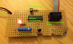
Prototype is built and operational. I've spent the last few days after work writing firmware for it, and have the basics up and running well. All of the coding and programming can be done using the Arduino development environment, changing LVC/HVC set points is just a matter of changing the two values and reprogramming.

Currently the firmware is set up to measure cell voltage once per second when it's below the HVC point. While charging and the cell voltage gets close to the HVC point, the update frequency goes up to about 4 times per second, during balance the update frequency rises to around 16 times/second. The LED flashes at difference rates during this process to signal status to the user.

I also wrote a routine to flash the LED in a pattern corresponding to the cell voltage. By shorting one of the attiny pins to ground (or pressing a button) the LED will flash to communicate voltage. For example, 3.45V would flash 3 times, pause, then flash 4 times, pause, then 5 times to indicate current voltage. When not doing anything, ie sitting in the bag, the microcontroller goes into power down mode to conserve power.

Not shown is an optoisolator to communicate with a master board (or Arduino if you so choose) or provide an LVC signal to interface with the motor controller or shutoff circuit. Since everything is configured in software, you can configure to your liking.

I'll keep updating this as I get the pcb laid out and have some boards built up. Initially I'm going to build 6S boards, although they can easily be used together for 12S, 24S, 37S, or any other size you might want. Unlike the previous version, this will be all through hole parts and configurable for any cell chemistry.

Balance current as I have it built is around 350mA, but can be adjusted be changing the resistor value. The resistor measures around 140F with an IR thermometer, and is hot to the touch but not enough to cause any burns unless you hold your finger on it for quite a while. The transistor is good up to around 600mA or so, but can easily be chained with something bigger to handle higher balance current.

Reprogramming can be done while connected to the battery, although it should not be done during charge.


Attachments

  • prototype.JPG
    prototype.JPG
    216 KB · Views: 4,868
Here is the base schematic, I only included one page since the others are identical. I've added a few components here and there to allow different build options. P201 should be left disconnected by default to allow programming while connected to a cell. P202 can be temporarily shorted to ground to trigger the voltage readout (via LED) routine.

I've been doing some power consumption testing to measure real world power consumption of the entire circuit. I've got a 0.47F, 5V super capacitor that I charge up to the HVC set point, then monitor voltage on the cap over time. Makes it pretty easy to calculate current consumption. I could use an actual micro amp meter, but I don't really trust the cheap ones and don't want to spend the money on a more expensive one. If anybody else has experience with this I'd be interested in hearing it.
 
Hi,
it's nice to see that you are making progress.
I have some questions to your circuit design:
Why are you using a PNP-Transistor instead of a MOSfet?
You included a Zener-diode in your design. Does it reduce voltage spikes induced by the cell?
I cannot read the type of the 1.2V reference you have. What did you choose?
Is the LED still shining bright enough at 2.5V battery voltage? What kind of lithium technology are you intending to use this BMS for?
Will you include a reverse voltage protection later on? Is a fuse neccesary?

with regards,

Johannes
 
Chuechco said:
Hi,
it's nice to see that you are making progress.
I have some questions to your circuit design:
Why are you using a PNP-Transistor instead of a MOSfet?
You included a Zener-diode in your design. Does it reduce voltage spikes induced by the cell?
I cannot read the type of the 1.2V reference you have. What did you choose?
Is the LED still shining bright enough at 2.5V battery voltage? What kind of lithium technology are you intending to use this BMS for?
Will you include a reverse voltage protection later on? Is a fuse neccesary?

with regards,

Johannes

I'm using a PNP for a few reasons. The primary one is that the voltage required to turn it on is much less than a FET. While it's not too hard to find FETs that will turn on at 3.5-4.0V, Vbe is around 0.65V for most BJTs and therefore simpler to source parts. FETs are also more prone to noise induced turn on, while BJTs are current controlled and easier to guarantee the state without extra components. BJTs are also generally cheaper and more available in through hole parts. In short, I could have used a FET and would have liked the higher current capability, but it was simpler and cheaper not to. After this version is finished and the kinks worked out I may do a higher balance current version. You could also easily swap out the balance resistor for a larger BJT and use them together in a darlington or sziklai pair.

The zener is primarily there to keep the voltage across any two cell terminals at or below that value, say if there was a broken cell wire somewhere. It guarantees the voltage stays evenly distributed. I'm not too worried about voltage spikes or over-voltage cells, because at over 5V on a cell the problem would not be in the BMS circuit.

The 1.2V reference is an LM285-1.2 from TI, operates down to 10 microamps and provides 1.235V with 1% tolerance over the whole temp range. I included the option to power it from one of the ATtiny ports to shut it off during sleep, although I may end up just leaving it powered all the time. I don't know if holding a port low to disable the reference will consume more power than it saves or not yet.

The LED is only typically turned on during balance, or if someone manually runs the routine to flash the cell voltage through it. In both of those cases the cell voltage is usually 3.0-4.0V. Red LEDs have a forward voltage of around 2V, so at 2.5V there's not a lot of current through it, but still enough to light it up in my experience. In the prototype I built I actually used a 1.5k resistor inline with the LED instead of 1k, and even at that level it's plenty bright.

I didn't include reverse voltage protection since in my opinion it's not necessary. Most BMSes I've seen don't include it, and in this design it would make measuring cell voltage less accurate due to the voltage drop across whatever protection scheme I was using. A fuse would be easy to add, but also not 100% necessary in my opinion.

Cell chemistry can be anything that lives in the range between 1.8V-5V, which is the range of the ATtiny84 I'm using and below the lower turn on limit of the zener. You could also use it on supercaps if you wanted. LVC and HVC limits are programmed in, so it can be used on LiFePO4 and then switched to Lipo just by reprogramming the chips. I included a programming header onboard, reprogramming only takes a few seconds per cell. I've changed the set points countless times during testing and firmware development. I'm using the Arduino IDE as well, which further simplifies things.

Good questions, hopefully I answered them sufficiently.
 
Quick question, if anybody has a couple 5Ah 6S packs that are close to dead that you would be willing to send me that would be a big help. Not looking to spend a lot, ideally just shipping costs, but I'd be willing to send you a couple of the BMS boards (pcb only) once they're done to say thanks.

I am considering including at least 2, maybe more headers for the balance pins so these can act as a parallel board in addition to the BMS functions.

PM me or post here if you have something.
 
If aiming at really low power consumption in the dozen uA or so I would be careful with the zener. I've never tested one into that low current, but I have one test where I took a 1N5231 5V1 zener to 3,58V and it draw 145uA.

I have a series shottky with the cell+ but the primary intent is not reverse polarity protection (although useful when installing) but to make sure small cell voltage deeps don't affect the micro (there's a 10uF cap after the diode).

I like your idea of using the LED to transmit cell voltage (data). Might steel it from you :)

As for the AVR internal Vref, I don't see any problems as I mentioned in the other thread. I can post my ADC configuration and reading code if you like, it's for the tinyX5 line but it's probably fully compatible.

You have no limiting resistor on your zener, what's your design rationale? I mean, the little zener can't hold down the voltage of a (few?) cell(s)...
 
Njay said:
If aiming at really low power consumption in the dozen uA or so I would be careful with the zener. I've never tested one into that low current, but I have one test where I took a 1N5231 5V1 zener to 3,58V and it draw 145uA.

I have a series shottky with the cell+ but the primary intent is not reverse polarity protection (although useful when installing) but to make sure small cell voltage deeps don't affect the micro (there's a 10uF cap after the diode).

I like your idea of using the LED to transmit cell voltage (data). Might steel it from you :)

As for the AVR internal Vref, I don't see any problems as I mentioned in the other thread. I can post my ADC configuration and reading code if you like, it's for the tinyX5 line but it's probably fully compatible.

You have no limiting resistor on your zener, what's your design rationale? I mean, the little zener can't hold down the voltage of a (few?) cell(s)...

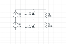
I specifically selected a low leakage zener (2uA @ 2V in theory), so hopefully it will be lower than the 1N series. I've got a test setup for measuring current set up, at some point this week I'm going to start isolating components to measure individual contribution to the total current draw over the voltage range. As far as reasoning behind the zeners, they're not intended to hold down cell voltage in the case of overcharge, the purpose is to protect the micros in case of a broken cell wire. It helps if you think of the BMS as a bunch of series resistors in parallel with the cells and zeners. Say all the cells are 4V, if a cell lead is broken, then you have the potential for up to 8V across one micro while another is drawing more current.

See the (simplified) representation below. 2x 4V cells in series, and the middle cell wire has broken. R2 represents a micro that's awake and doing something, R1 is a sleeping micro. R2 will effectively "pull" the positive terminal of R1 up towards itself due to the lower effective resistance. The zeners protect against this by clamping the voltage. It's also a potential issue when plugging a pack into the BMS. Inevitably some cells will be connected before others just due to differences in each pin, angle of insertion,etc. Even a few ms over voltage is enough to damage the microcontroller.

2-cells-simplified.png

Feel free to steal the voltage LED flashing idea, the code is incredibly simple, I can post the routine if you want it. Otherwise the whole firmware code will be open source anyway. I plan on using one of the empty pins attached to a pin change interrupt to trigger the code.

I'd be interested in seeing your ADC Vref config code, I have some tinyx5s sitting around as well I can try it on. It wouldn't be hard to port either.
 
Ok, so it's because you have all monitors on the same PCB and 2 adjacent monitors share the wire into the cell, right?

Thank you for the code offer, I was only talking about the concept, not sure what I'll do but who knows I might come about to use it.

This is the code for the ADC (CPU is running at 4MHz internal RC clock generator):

Initialization
Code:
    // Select internal 1.1V ADC Vref.
    ADMUX |= _BV(REFS1);
    // Fadc = 125KHz
    ADCSRA |= _BV(ADPS2) | _BV(ADPS0);  // sysclock divided by 32 -> 4MHz / 32 = 125KHz
    // Disable digital input buffer on the ADC inputs used for temp and
    // cellVoltage, to reduce power consumption.
    DIDR0 |= _BV(ADC1D) | _BV(ADC3D);

    // Sleep mode is always ON and set to default reset-time sleep mode (no configuration done)

Reading
Code:
EMPTY_INTERRUPT(ADC_vect)        // will just do an IRET or similar

// Our own sleep function. AVR libc's sleep_mode() will always enable sleep mode on
// entry and disable it on exit, which takes up 4 instructions.
static inline void sleep (void)
{
    asm volatile("sleep");
}

// Read an ADC channel. ADC must be enabled on call to this routine.
static uint16_t ReadAdc (uint8_t channel)
{
    byte  prevSREG;
    uint16_t  val;

    // Set channel
    ADMUX = (ADMUX & 0xf0) | channel;
    //set_sleep_mode(SLEEP_MODE_ADC);   // can't use this, doesn't allow timer1 to operate
    // Enable intrs, ADC. Conversion starts automatically when entering sleep mode.
    // In 2 steps + nop to give it extra clocks for better mux input stabilization.
    ADCSRA |= _BV(ADIE);
    ADCSRA |= _BV(ADSC);
    asm volatile("nop");

    // Wait end-of-conversion. The ADC interrupt will unblock sleep.
    do sleep();
    while (ADCSRA & _BV(ADSC));     // wait for the bit to go to zero

    //set_sleep_mode(SLEEP_MODE_IDLE);

    // Read the value
    prevSREG = SREG;
    cli();
    val = ADCW;
    SREG = prevSREG;
    ADCSRA &= ~(_BV(ADIE));    // disable ADC interrupt
    return val;
}

I actually use it roughly like this:

Code:
ADCSRA |= _BV(ADEN);        // ADC on
// Read cell voltage, average of 2 readings
uint16_t  vcell = ReadAdc(eVcell);        // eVcell is an enum with the channel's number
vcell = (vcell + ReadAdc(eVcell)) / 2;
// do other readings here, like the temperature...
ADCSRA &= ~_BV(ADEN);        // ADC off
 
Njay said:
Ok, so it's because you have all monitors on the same PCB and 2 adjacent monitors share the wire into the cell, right?

Exactly. If it were only one cell I wouldn't need the zener. That's how I built the prototype for doing the firmware development.

Thanks for the code, after a quick look I don't see you doing anything fundamentally different than I was, I'll have to try it out myself and see if I'm missing something. I see you disabled the digital input buffers, did you see any significant power reduction that way?
 
dmwahl said:
I see you disabled the digital input buffers, did you see any significant power reduction that way?
Never measured the difference, I just disabled everything I could/knew. I was/am aiming at few uA sleep mode consumption.
 
Njay said:
dmwahl said:
I see you disabled the digital input buffers, did you see any significant power reduction that way?
Never measured the difference, I just disabled everything I could/knew. I was/am aiming at few uA sleep mode consumption.
What was the project?

I've taken a few current measurements and I'm averaging around 200uA average current regardless of how often I come out of sleep to measure the cell voltage. Sleep mode is power down, brown out is disabled, along with all the other peripherals except the watchdog timer to wake it back up. 200 microamps is higher than I had hoped but still not bad, I suspect most of it is leakage through the pnp transistor.
 
The project is a per-cell monitor of voltage and temp. I haven't done an analysis on consumption yet, although I know it is currently "too high".
 
Alan B said:
200 uA seems high. Did you turn off the analog reference, ADCs, etc? Some of the AVRs will go down to 0.1uA, most will go to a few uA when powered down.

Yep, turned that all off. Both timers, ADC, USI, and brown-out detector.The 0.1uA number is only with the watchdog disabled, since I need to wake periodically my theoretical minimum is more like 4-8uA from the micro itself.

My theory (untested so far) is that the AVR's internal pullup that is effectively connected between the base and emitter isn't strong enough or is very slightly biased and allowing some current to flow. I'm going to try connecting an external pullup and see if that helps.

Also worth noting is that 10-30uA is from the 1.2V reference, it has a 75k resistor in series and will pull around 10-30uA all the time. I am going to try connecting the reference through an I/O port to turn it off when not reading, but I haven't yet determined if that will be a net savings or not.
 
Supplying the reference from an output should be a savings, when you tristate it or set it low there will be no current flow.

As others have mentioned the internal reference is fine if calibrated, good enough for the 10 bit ADCs anyway, so the external reference is not needed, but when turning the ADC and internal reference on and selecting it some time is required and some readings should be discarded before taking readings for use, and averaging a number of readings is also a good idea for many reasons.
 
Try to get rid of the external reference if calibrating the internal one is not too much work for your production step plans.

In my board the external devices I have that consume power are the temp sensor (6uA) and the resistor divider (320uA@3.2V). Both will be switchable ON/OFF. Then it's only the CPU, but I need at least 4MHz and that takes power even sleeping frequently; so my strategy will be:

1) Micro powers up with 1MHz clock or less, everything off except RX pin interrupt, then enter sleep as deep as possible. It should come out of sleep only on activity on the RX line. This is the state it will be when not in use (the monitor will always be connected to the cell; we're talking LiFePO4 40Ah+ cells).
2) On the 1st RX activity (the system console will "shake" the RX line to wake up all monitors) switch the clock to 4MHz and turn on the relevant stuff (timer, ...), including the watchdog, and it's now ready to answer requests.
3) On every received packet kick the watchdog. The console will poll the monitors several times a second, so the watchdog will be quiet during "normal usage".
4) If the watchdog expires the micro resets and gets back to 1), the low power state.

I don't have enough space for this on the tiny25V I'm using now but I'll have on the tiny44. Consuming very little is critical when the system is not in use, so I'm focusing on that while relaxing the power saving requirements "at rest", to prevent quick "self discharge" of the cell and ruining it.
 
Alan B said:
Supplying the reference from an output should be a savings, when you tristate it or set it low there will be no current flow.

As others have mentioned the internal reference is fine if calibrated, good enough for the 10 bit ADCs anyway, so the external reference is not needed, but when turning the ADC and internal reference on and selecting it some time is required and some readings should be discarded before taking readings for use, and averaging a number of readings is also a good idea for many reasons.

Njay said:
Try to get rid of the external reference if calibrating the internal one is not too much work for your production step plans.

In my board the external devices I have that consume power are the temp sensor (6uA) and the resistor divider (320uA@3.2V). Both will be switchable ON/OFF. Then it's only the CPU, but I need at least 4MHz and that takes power even sleeping frequently; so my strategy will be:

1) Micro powers up with 1MHz clock or less, everything off except RX pin interrupt, then enter sleep as deep as possible. It should come out of sleep only on activity on the RX line. This is the state it will be when not in use (the monitor will always be connected to the cell; we're talking LiFePO4 40Ah+ cells).
2) On the 1st RX activity (the system console will "shake" the RX line to wake up all monitors) switch the clock to 4MHz and turn on the relevant stuff (timer, ...), including the watchdog, and it's now ready to answer requests.
3) On every received packet kick the watchdog. The console will poll the monitors several times a second, so the watchdog will be quiet during "normal usage".
4) If the watchdog expires the micro resets and gets back to 1), the low power state.

I don't have enough space for this on the tiny25V I'm using now but I'll have on the tiny44. Consuming very little is critical when the system is not in use, so I'm focusing on that while relaxing the power saving requirements "at rest", to prevent quick "self discharge" of the cell and ruining it.

I want to avoid having to calibrate the internal ref, or at least give the option for an external one. As it stands now, the option exists to use either the internal or external reference. I am definitely going to experiment with calibrating the internal ref, but for the people who would rather just spend another 50-60 cents per cell the external ref is a good option and very reliable.

I'm planning on oversampling to at least 12-bit resolution when close to HVC, although when far away from the cell limits I don't see much benefit. Maybe to 11-bit to smooth things out for logging.

Thanks for the feedback and suggestions.
 
Njay said:
Try to get rid of the external reference if calibrating the internal one is not too much work for your production step plans.

In my board the external devices I have that consume power are the temp sensor (6uA) and the resistor divider (320uA@3.2V). Both will be switchable ON/OFF. Then it's only the CPU, but I need at least 4MHz and that takes power even sleeping frequently; so my strategy will be:

1) Micro powers up with 1MHz clock or less, everything off except RX pin interrupt, then enter sleep as deep as possible. It should come out of sleep only on activity on the RX line. This is the state it will be when not in use (the monitor will always be connected to the cell; we're talking LiFePO4 40Ah+ cells).
2) On the 1st RX activity (the system console will "shake" the RX line to wake up all monitors) switch the clock to 4MHz and turn on the relevant stuff (timer, ...), including the watchdog, and it's now ready to answer requests.
3) On every received packet kick the watchdog. The console will poll the monitors several times a second, so the watchdog will be quiet during "normal usage".
4) If the watchdog expires the micro resets and gets back to 1), the low power state.

I don't have enough space for this on the tiny25V I'm using now but I'll have on the tiny44. Consuming very little is critical when the system is not in use, so I'm focusing on that while relaxing the power saving requirements "at rest", to prevent quick "self discharge" of the cell and ruining it.

I'm curious about this, what protocol are you using for cell communication? How do you prevent conflicts between cell monitors trying to send data all at once? (Assuming you are using one data bus and not individual lines or select pins for each cell.) Clever to use the master to wake the cells.
 
It's a oneway ringbus. Console (master) connects to 1st monitor, then 1st monitor to 2nd monitor, ... until last monitor connects "back" to console.

Messages are addressed, so if a monitor receives one which is not for itself (there's also a "broadcast" address) it just forwards it. In the planned strategy described above, when the console "shakes" the bus to wakeup the monitors it is in fact shacking the 1st monitor; then the 1st monitor will shake the next one on the ring and so on.

The protocol at the link layer was implemented in sw, roughly described troughout here, here and here.
 
Njay said:
It's a oneway ringbus. Console (master) connects to 1st monitor, then 1st monitor to 2nd monitor, ... until last monitor connects "back" to console.

Messages are addressed, so if a monitor receives one which is not for itself (there's also a "broadcast" address) it just forwards it. In the planned strategy described above, when the console "shakes" the bus to wakeup the monitors it is in fact shacking the 1st monitor; then the 1st monitor will shake the next one on the ring and so on.

The protocol at the link layer was implemented in sw, roughly described troughout here, here and here.

Thanks, I will read through those in more detail tonight. Should give my wife something else to wonder about what the heck I'm doing :)
 
Back
Top