How to Repair a Standard 42V Lithium Ion Charger/PowerSupply

sapo

1 mW
Joined
Sep 21, 2011
Messages
18
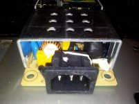
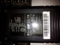
I PM'd a member to ask how he went about repairing failed charger power supplies. I mean the ones that come in a black plastic box like a laptop power supply. I suspect that they output a stable source of 42V and the circuitry inside the battery [BMS] does all the cell balancing and special charging methods depending on the actual battery's lithium chemistry.

Anyway the member replied as follows and suggested I start a Topic.

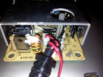
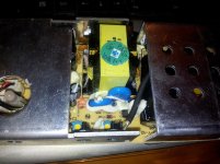
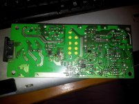
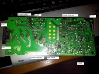
the first thing is to make sure the board is getting power and the fuse is not blown, then look for the rectified DC on the input caps, which comes off the rectifier bridge. then look for voltage in the back end by measuring on the output of the schottky diode to see if the charger is pushing current into the back end.

open the chargers and take pictures too. but check for voltages first and if no voltage then see if the fuse is blown. that was the most common problem i found on all these charger returns i have here.


OK great, but when I had a look in one I could not recognise anything that looked like a fuse... so can anyone please tell me what size/shape/color component I should be looking for?
 
Here are the photos. Could you please describe what you recognise?
 

Attachments

  • AC end.jpg
    AC end.jpg
    139.3 KB · Views: 2,724
  • DC end.jpg
    DC end.jpg
    129.3 KB · Views: 2,719
  • mid section.jpg
    mid section.jpg
    218.1 KB · Views: 2,724
  • tracks.jpg
    tracks.jpg
    217.8 KB · Views: 2,722
  • label.jpg
    label.jpg
    256.8 KB · Views: 3,678
on the AC end, just to the left of the plug you can see a fuse covered with heat shrink tubing. there is a label that says F1 next to it.

using you voltmeter set to the ohmmeter scale, measure the resistance from one end of that fuse to the other. it should be 0 ohms, or continuous.

on the back end i can see a relay in that little black box on the left. this means the charger will only put out voltage to the output wires when it is connected to the battery, with the right polarity. the relay is there to protect the charger from reversing the battery on the charger output. you will not see any voltage on the output if you measure there with the voltmeter since the relay is turned off until the batter is connected. then you can measure the output voltage, which will be the same as the battery voltage then.

the middle portion show two blue cermet trimpots with the yellow dial in the middle. one of those will adjust the output voltage, and the other will adjust the output currrent so if you wanted to hack the voltage or current up, that is where you would tweak it.

if you have no lights coming on at all when you plug in then i expect the fuse is blown open.

i have to order some of the little fuses yet to fix one of greg's chargers so lemme know if that one is dead and i can send you the ebay link for some replacements.
 
That is excellent dnmun. Thanks for that. Do you have any circuit diagram or block diagram illustrating the functional structure of this kind of device.

I am definitely interested in the fuse link. I am sure I will need more in the future. Would you expect a different fuse for a 2 A and a 3 A supply?

So is the fuse shrink wrapped to reduce the risk of shock?

Am I right in thinking that the detailed charge control is done by the BMS in the battery and that this black box in merely a power supply providing the maximum allowable voltage for the specific battery?
 
nope, i don't have any diagrams.

did you measure the continuity of the fuse and it was open?

http://www.ebay.com/itm/190536802078?ssPageName=STRK:MEWAX:IT&_trksid=p3984.m1438.l2649
 
you can see the capacitor in the middle section photo. it is the big black one under the heat sink so see if you can measure the voltage between each leg of that capacitor. you can reach them underneath if you look at where the leads are soldered into the pcb.

also when you look at the traces picture. there is a small dogleg that comes off one of the transformer leads in the back end, in the middle upper right, and the trace goes over to a three terminal device called a schottky diode. the two outside legs are tied to the same trace as you see and the middle trace goes off towards the output + terminal.

find the negative output spot where the wire comes off the pcb, use that as ground in the back end to measure.

if there is voltage in the front end then measure with the red probe the DC voltage on the middle pin of that schottky diode using the negative output for the black probe.

do this while it is active electrically. we can test the diode later when it is off.
 
yes, the switch mode power supplies have a front end where the high voltage lives, then that voltage drives currents in the transformer that resulst in current going out the other side of the transformer into the back end. it goes from the transformer through the schottky diode into the battery.
 
The voltage across the big capacitor was not stable DC. It seemed to polarized but fluctuating wildly on my multimeter.

There was zero DC voltage at the Schottky diode.

AC was passing through the fuse alright.
 
the DC on the front end is noisy coming off of the rectifier diode bridge. did it measure 170V?

you can test the diodes in the rectifier bridge to see if one is burnt out.

in the upper left corner on the traces picture there are 4 legs of the rectifier diode soldered into the pcb. you can see the diode bridge on top screwed to the heat sink.

with the power off, use your diode tester on your votmeter to test each pin with respect to each of the others, and see what the forward bias is and then reverse the probes and it should be open circuit, inifnite resistance. unplug it first though. measure at the pins on the underside. if the forward bias on one of the diodes is 0V then it is shorted. normal forward bias would be about .45V or so.
 
The voltage at the capacitor was 154 no 273 no 325 no 50 no etc but faster. :lol:

Ok I will check the diodes l8tr.
thanks.
 
if you had DC voltage i would guess the diodes are ok. but it is useful for you to test them since you wanna get feel for what the thing does when it works, because this is how all these little charger bricks are made.

yours is neat because you can hack the current and voltage easily. so it can be used for other voltage packs. it needs a fan though to hack the current up a bunch. but first get it fixed.

so you should test the mosfet to see if it is shorted or open. can you see it by looking under the heat sink and does it look smokey and have cracks in the plastic?

you can test it with your voltmeter on the legs where it is soldered into the pcb.

you can see it next to the diode bridge, and the solder trace runs from the end of the rectifier diode (negative end of the rectifier diode bridge) right to the source leg of the mosfet. and the drain leg runs out to the transformer.

so what is happening is that when that mosfet turns on, it conducts current from the high voltage on the capacitor through the transformer winding and through the drain leg to the source leg and from the source leg over to the ground on the rectifier diode bridge. make sense?

that current going through the transformer induces current in the secondary windings and the current in the secondary windings goes out of the transformer and through the schottky diode and into the battery.

the switching mosfet in the front end is controlled by that little 8 pin IC next to it and you can follow the trace that goes over to the gate of the mosfet from the upper right corner of that little SOIC.

in the other corner on the second pin is where the feedback goes into that pwm IC current controller. so when the back end wants current, it turns on that opto transistor that the feedback pin is connected to.

they have to use an opto transistor to isolate the front end from the back end because of the different voltages and sides of the transformer really.

but getting back to the switching mosfet, you can check it by using the diode function on the voltmeter, and checking to see if there is a body diode in the mosfet. or if it has shorted or blown open.

you do that by placing the red probe on the source leg and the black probe on the drain leg (while the charger is off) and measure the forward bias. then once you measure the body diode, should about .4V, then reverse the leads, put the black lead on the source leg and the red lead on the drain and measure the resistance of the diode. it should be open, or infinite resistance when measured on the diode tester.

so that would tell you if the mosfet works.

in the 'middle' picture i think that black wire screwed to the heat sheild is tied to the negative output, or ground. if you look right underneath it on the pcb there is one end of the opto transistor visible, and other end is covered by goop. that is the opto transistor that carries the feedback from the back end to the pwm IC current controller in the front end. the feedback voltage on the output of that opto is usually .3V on the transistor end. you can google up the fairchild 817B data sheet to see how it works.

http://www.fairchildsemi.com/ds/FO/FOD817A.pdf

but that black wire and the heat shields might be at the AC ground too because that has a three pin plug i think. maybe you can see.
 
Hey great information.
If you could elaborate more on the best way of beefing up power outout it would be much appriciated
 
on this charger there is that blue trimpot with the yellow dial that is part of the shunt so you can just tweak the power up by turning the trimpot down. the other is for the output voltage.

after looking at the front end picture i can see that black wire that screws onto the heat sinks comes off the AC ground pin at the plug. so that is how they ground the rf shielding to meet the radiative guidelines.

it looks like the heat sink is mounted on the pcb and is there during reflow so all the parts inside the heatshield are all placed and mounted, then the heat sinks mounted in their holes, then the entire pcb with the heat sink on top goes through reflow.

there is no need to mount any other parts after reflow so the heat sink is not in the way, and the two trimpots are exposed there but the white potting goop must be added afterwards. to remove any of the parts like the rectifier diode or the mosfet or schottky diode which are bolted to the heat sink you would have to unsolder those tabs that hold the heat sink on, unscrew the device attached to it and remove the heat sink to reach the mosfet or diode.

so all those parts must have been attached to the heat sink during reflow or nobody could reach the nut inside.

he said he wanted some diagrams, so maybe that helps. but all the charger bricks are essentially identical.
 
Are the little yellow components eg C4 capacitors?
So is the Opto coupler bridging across the slot in the board near C16?
Looking at the mosfet pins under the board, do they go from the AC end: source drain gate?

the bridge diodes test okay.

the mosfet tests okay. the source has a forward bias towards the drain and the gate. All other directions are high impedance.

are you saying that there should be a dc measurement of .3 volts on the ac side of the opto coupler?

Wouldn't you expect a stable dc voltage across the big capacitor?
 
to be honest i don't know what to expect. i have never done any of this stuff before. just been teaching myself as i go along. there are smart people around who know.

but i assumed it is just the meter trying to measure the voltage and there is electrical noise it sees that give it a range of readings.

the .3V is what i remember as the feedback voltage that the pwm IC needed on the feedback pen, from the spec sheet. i think it was the 3842 pdf i read.

but since you have voltage present on the capacitor it should be switched through the transformer.

you should see voltage on the center pin of the schottky diode. thing should be working.

if you read about common cathode schottky diodes you will see how the current goes in through each side anode and comes out the center cathode pin. that pin has to have the output voltage on it.

you can test the schottky by doing the diode test on it too.
 
The Schottky diode IC is a dead short.
It is MBR10200CT and by coincidence I just bought some MBR20100CT for a solar project.
The web implies that it is 10 A/ 200 V versus 20 A / 100 V.

Should be OK I guess. Hopefully that will solve the problem. Thanks!!!

I once heard the white thermal heat sinking paste is quite toxic or carcinogenic. Do you know anything about that. I am trying not to get it on my skin.
 
For everyone's benefit I have attached the photo of the tracks/traces with annotations locating the key components discussed here.
Good luck!
sapo
 

Attachments

  • tracks - annotated.jpg
    tracks - annotated.jpg
    228.1 KB · Views: 2,715
that is really helpful for the others to follow what you did. the pin out on the pwm IC is different from what i expected but you can see the gate drive trace going up to the mosfet, it has a current limiting resistor then it goes up to where the zener diode DA goes between the gate trace and ground. that little resistor Rd is there to ground the gate when the device turns off each cycle. the oscillator on these pwm ICs is around 300khz. it is adjustable by changing R7 i think.

the IC current controller has to know how much current flowed through the transformer during each cycle in order to know when to turn off the mosfet so it follows the voltage spike on big power resistor between the source and the ground on the upper side. usually a 5W resistor, around 4-5 ohms. you can see where the legs are soldered into the pcb between the source leg and the ground trace.

the voltage signal from the source leg comes back to the pwm IC on that jumper across the slot in the pcb and passes right above R9 on the way back to the pwm IC, and the jumper right above it will be ground and you can see the ground run up to the IC and there is a cap Ca between the ground and the high voltage trace coming over through R1 and R2. i think they read 123 so that would 24k ohms across 170V so 7.5mA current supplied to the voltage regulator inside the pwm IC.

the schottky will appear as shorted in one direction so you have to test the diode function between the anode and cathode.

there is also another passive circuit element between the anode and cathode on the schottky diode. you will see it as a ceramic capacitor in series with a big power resistor connected between the anode and the cathode of the schottky. that is called a 'snubber' and it absorbs the high frequency (voltage) ringing on the the output from the cathode. that is a low ohm resistor too so if the capacitor in the snubber is shorted, it can also appear as a shorted schottky. maybe R14 and R14A are part of the snubber. and the ceramic cap is on those two legs sticking down into the trace on end of R14, goes over to where the transformer lead is soldered in to the trace running over to the double anodes.

does that make sense? but i bet it is the diode that shorted. getting it out will be a bitch. that heat sink is in the way but if you can find a way to reach the nut that holds it to the heat sink then unscrew it and push it off of the heat sink in case it might be shorted through the heat sink so you could again retest it while pushed away from the heat sink but it is likely suspect now.

as i recall from the middle picture the diode is almost at the opening so you should be able to get it out once you are able to desolder the legs and use a solder sucker or the whack technique to get the solder outa the holes around the diode legs. use some solder wick too in order to remove all the solder from the holes so the diode will be free and come loose so you can pluck it up through that gap between the heat sink/shields. then put the new diode back, getting the nut on the end of the screw again will be a test of your manhood. don't get too frustrated and break it now, hehe.

double stick tape on the end of a wire loop to hold the nut behind the diode when you run the screw through. don't snug the screw too tight, more thermal heat sink grease needed too, that stuff better not be toxic. just zinc oxide in silicone oil.

also one other thing about the schottky diodes. you will notice in the advertising they talk about ultra fast and hyper ultra fast diodes and price of the diode goes up with the speed. the reason you want the diode to turn off fast is so that the current sucked through the diode as the diode shuts off is very small, short time to turn off means less time carrying current as the diode turns off. so you don't use just any old rectifier diode but i have seen a lot of MBRs used. the chinese seem to always use a 200V hyperfast diode.
 
I forgot to say that the heat sink has a cut-away directly above the Schottky IC. It must be a regular occurrence. Made removal easy.

I used the 'push the hot iron tip down on the leg end many times' technique, moving from leg to leg until it came out before the board got totally botched. Must keep an eye out for a wick...

Love the way your brain flows down those wires.

Cheers. :D
 
Back
Top