ElectricGod
10 MW
A couple of months ago I did a review of the Chargery C1042B. I was pretty scathing since those chargers are giant piles of garbage. I still wanted a high wattage, many cell charger so I bought this iCharger 4010. I paid $300 for it...so not exactly inexpensive. One of the things I was curious about is if it had any of the issues the C1042B has. I can emphatically say that it does NOT have any of them.

1. The LCD is a lot brighter, clearer and higher resolution. It can be viewed in direct sunlight and while not an IPS LCD, it's a decent TN display that can be read at angles.


2. The charger can be left connected to a battery pack for weeks at a time and NOT run down the cells. It balances well and there is no hint of over charging one cell over another.
3. The charger is a good bit smaller than the C1042B, but then it has no internal power supply.
4. The design of the charger is neat and clean with no extraneous inter connections. It's far better designed than the C4012B...which is just garbage. If there is one thing I like more about the Chargery C4012B it's the aluminum shell.
It comes with these cables and balance boards.

I do have a few minor complaints. Otherwise...this is a brilliant charger.
1. You need your own PSU. I already had one so that was not a big concern to me. However for a lot of folks dropping $300+ for the charger and then buying a $75 PSU makes this a fairly expensive purchase.
2. The large capacitors on the board are not secured except by their legs.
3. The ribbon cable from the main board to the top cover board is too short and has fairly fragile connectors.
4. For a charger this expensive it ought to have BT, android/IOS app and a PC app. It has none.
5. THe power input isn't an XT90...which are cheap and super common.
6. The 2 power output cables had bare ends. I had to add my own XT90's.
So then...onto some exterior pictures...


The bottom comes off with 5 screws and then slides off easily to reveal this monster heat sink.

The top is held to the board via 2 screws. Once they are removed there's this short ribbon cable to disconnect. It's connectors are quite tiny and fragile so it's good to NOT pull on it in any way. The ribbon cable is about 2" long. It would be a bit easier to unplug if this cable was another inch longer.

Once the top is pulled off there is a small board that has the switches on it and a smaller ribbon that goes to the LCD.

The CPU says "ARM" on it...so I can make a fairly good guess what this CPU is based on it's pinout and and shape. Otherwise...they have etched off the top of the CPU. Notice that tiny connector. This is where the ribbon cable to the top cover connects. It's all of 1/2" long and that black plastic part is super fragile.

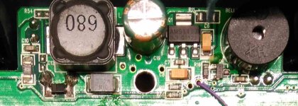
A few pics of the top side of the charger main board...


The underside of the main board...


The board is held down to the heat sink by 8 screws. All the screws are strategically placed at mosfets or where they provide the best support and clamping pressure to the mosfets and heat sink.


The bottom of the board.

The heat sink has 2 pads of thermal gap filler that sink heat away from the 20 balancing transistors. The 11 places for the mosfets have glass insulators with heat grease on them.

This is the balancing transistors. They have fairly large resistors underneath them. I expect 2A balance current is quite possible.


The charging logic.

All the mosfets have very short legs and they are reinforced with solder. This ought to make them handle the maximum current possible with the best heat transfer.

A small DC-DC converter for powering the logic.

1. The LCD is a lot brighter, clearer and higher resolution. It can be viewed in direct sunlight and while not an IPS LCD, it's a decent TN display that can be read at angles.
2. The charger can be left connected to a battery pack for weeks at a time and NOT run down the cells. It balances well and there is no hint of over charging one cell over another.
3. The charger is a good bit smaller than the C1042B, but then it has no internal power supply.
4. The design of the charger is neat and clean with no extraneous inter connections. It's far better designed than the C4012B...which is just garbage. If there is one thing I like more about the Chargery C4012B it's the aluminum shell.
It comes with these cables and balance boards.
I do have a few minor complaints. Otherwise...this is a brilliant charger.
1. You need your own PSU. I already had one so that was not a big concern to me. However for a lot of folks dropping $300+ for the charger and then buying a $75 PSU makes this a fairly expensive purchase.
2. The large capacitors on the board are not secured except by their legs.
3. The ribbon cable from the main board to the top cover board is too short and has fairly fragile connectors.
4. For a charger this expensive it ought to have BT, android/IOS app and a PC app. It has none.
5. THe power input isn't an XT90...which are cheap and super common.
6. The 2 power output cables had bare ends. I had to add my own XT90's.
So then...onto some exterior pictures...
The bottom comes off with 5 screws and then slides off easily to reveal this monster heat sink.
The top is held to the board via 2 screws. Once they are removed there's this short ribbon cable to disconnect. It's connectors are quite tiny and fragile so it's good to NOT pull on it in any way. The ribbon cable is about 2" long. It would be a bit easier to unplug if this cable was another inch longer.
Once the top is pulled off there is a small board that has the switches on it and a smaller ribbon that goes to the LCD.
The CPU says "ARM" on it...so I can make a fairly good guess what this CPU is based on it's pinout and and shape. Otherwise...they have etched off the top of the CPU. Notice that tiny connector. This is where the ribbon cable to the top cover connects. It's all of 1/2" long and that black plastic part is super fragile.
A few pics of the top side of the charger main board...
The underside of the main board...
The board is held down to the heat sink by 8 screws. All the screws are strategically placed at mosfets or where they provide the best support and clamping pressure to the mosfets and heat sink.
The bottom of the board.
The heat sink has 2 pads of thermal gap filler that sink heat away from the 20 balancing transistors. The 11 places for the mosfets have glass insulators with heat grease on them.
This is the balancing transistors. They have fairly large resistors underneath them. I expect 2A balance current is quite possible.
The charging logic.
All the mosfets have very short legs and they are reinforced with solder. This ought to make them handle the maximum current possible with the best heat transfer.
A small DC-DC converter for powering the logic.
") I was lucky i think considering what I was doing with it
I was lucky i think considering what I was doing with it