As we are busy anyway, lets continue with my view of gate resistors.
View attachment 3
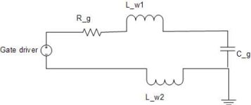
Going from left to right we have the gate driver, the gate resistor R_g, the wiring inductances of the
connections between the driver IC and FET (L_w1 and L_w2) and then the FET. I only drew the low side driver
but the high side is of course the same. Now the gate side of the FET can be modelled by a capacitor C_g.
Then we get this equivalent:

This is again one of those LCR circuits that has a certain ringing frequency from the L & C with damping
coming from the R. The main difference with the drain / source side snubber circuit is that on the
gate side the currents are relatively low and it is therefore possible to add a resistor R_g in the signal
path (I mean, you're not going to add a resistor in the drain with all those amp we want there, so an
alternative method is used there by inserting the snubber cap).
The equivalent circuit does not model the Miller plateau but this is not necessary for the gate overshoot we're
interested in.
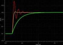
Again some simulation results:

Here the red curve has a low gate resistance, the yellow an intermediate and the green a high gate resistance.
Again, with no or too small a resistance there's insufficient damping so you get the ringing. What I typically
do is experiment a little with resistor values untill I get the yellow curve. The green curve is slow and is
kind of what ZombieSS found in the china controllers. Note that the red curve goes over the 20V allowed for
a typical FETs gate voltage, instand death and blue smoke territory. For my bicycle (done 250 km so far never
blown a FET) I use NCP5181 gate drivers that have a small built-in gate resistor. I actually have no gate resistor
on my PCB as the built-in resistor already gives me the yellow curve.
Looking again at the circuit in more detail, I deliberately placed the ground at the FET and placed L_w2 inbetween
the FET and the gate driver circuit. This is actually a realistic situation and is specifically mentioned in the
application notes that International Rectifier distributes.
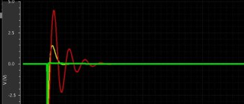
Lets look at the node inbetween L_w2 and the gate driver.

Ignoring the initial spike down (no energy content) we see that the red curve has (the one with the too low
gate resistance) has a big swing down to around -2.5 while the green and yellow only go maybe 100mV below
ground. This swing down is also specified in the spec of the gate driver IC's and is typically not allowed to
be more than about 700 mV below ground. The red curve would blow up the gate driver IC...


